CY8C21x34 Final Data Sheet
3. Electrical Specifications
3.1
Absolute Maximum Ratings
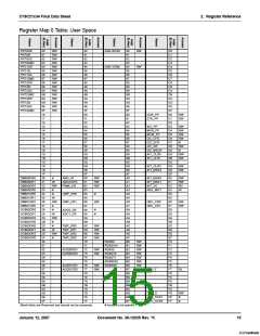
Table 3-2. Absolute Maximum Ratings
Symbol
Description
Min
-55
Typ
Max
+100
Units
Notes
o
o
T
Storage Temperature
25
Higher storage temperatures will reduce data
retention time. Recommended storage temper-
C
STG
o
o
ature is +25 C ± 25 C. Extended duration stor-
o
age temperatures above 65 C will degrade
reliability.
T
A
Ambient Temperature with Power Applied
Supply Voltage on Vdd Relative to Vss
DC Input Voltage
-40
–
–
–
–
–
–
–
+85
C
Vdd
-0.5
+6.0
V
V
V
Vss - 0.5
Vss - 0.5
-25
Vdd + 0.5
Vdd + 0.5
+50
V
IO
DC Voltage Applied to Tri-state
Maximum Current into any Port Pin
Electro Static Discharge Voltage
Latch-up Current
V
IOZ
MIO
I
mA
V
ESD
LU
2000
–
–
Human Body Model ESD.
200
mA
3.2
Operating Temperature
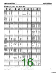
Table 3-3. Operating Temperature
Symbol
Description
Min
-40
Typ
Max
+85
Units
Notes
o
o
T
A
Ambient Temperature
Junction Temperature
–
–
C
C
T
-40
+100
The temperature rise from ambient to junction is
package specific. See “Thermal Impedances”
on page 36. The user must limit the power con-
sumption to comply with this requirement.
J
3.3
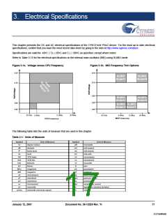
DC Electrical Characteristics
3.3.1
DC Chip-Level Specifications
The following table lists guaranteed maximum and minimum specifications for the voltage and temperature ranges: 4.75V to 5.25V
and -40°C ≤ TA ≤ 85°C, 3.0V to 3.6V and -40°C ≤ TA ≤ 85°C, or 2.4V to 3.0V and -40°C ≤ TA ≤ 85°C, respectively. Typical parameters
apply to 5V, 3.3V, or 2.7V at 25°C and are for design guidance only.
Table 3-4. DC Chip-Level Specifications
Symbol
Description
Min
2.40
Typ
Max
5.25
Units
Notes
Vdd
Supply Voltage
–
3
V
See table titled “DC POR and LVD Specifica-
tions” on page 22.
o
I
Supply Current, IMO = 24 MHz
–
–
–
4
mA
mA
mA
Conditions are Vdd = 5.0V, T = 25 C, CPU = 3
A
MHz, 48 MHz disabled. VC1 = 1.5 MHz, VC2 =
93.75 kHz, VC3 = 0.366 kHz.
DD
o
I
Supply Current, IMO = 6 MHz using SLIMO mode.
Supply Current, IMO = 6 MHz using SLIMO mode.
1.2
1.1
2
Conditions are Vdd = 3.3V, T = 25 C, CPU = 3
A
MHz, clock doubler disabled. VC1 = 375 kHz,
VC2 = 23.4 kHz, VC3 = 0.091 kHz.
DD3
o
I
1.5
Conditions are Vdd = 2.55V, T = 25 C, CPU = 3
A
DD27
MHz, clock doubler disabled. VC1 = 375 kHz,
VC2 = 23.4 kHz, VC3 = 0.091 kHz.
o
o
I
Sleep (Mode) Current with POR, LVD, Sleep Timer, WDT,
and internal slow oscillator active. Mid temperature range.
–
2.6
4.
µA
µA
V
Vdd = 2.55V, 0 C ≤ T ≤ 40 C.
SB27
A
o
o
I
SB
Sleep (Mode) Current with POR, LVD, Sleep Timer, WDT,
and internal slow oscillator active.
–
2.8
5
Vdd = 3.3V, -40 C ≤ T ≤ 85 C.
A
V
Reference Voltage (Bandgap)
1.28
1.30
1.32
Trimmed for appropriate Vdd. Vdd = 3.0V to
5.25V.
REF
January 12, 2007
Document No. 38-12025 Rev. *K
18
[+] Feedback

 CYPRESS [ CYPRESS ]