CY8C21x34 Final Data Sheet
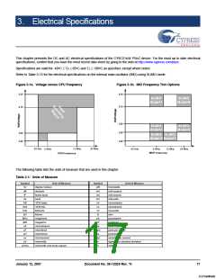
3. Electrical Specifications
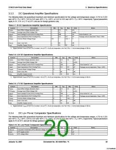
3.3.3
DC Operational Amplifier Specifications
The following tables list guaranteed maximum and minimum specifications for the voltage and temperature ranges: 4.75V to 5.25V
and -40°C ≤ TA ≤ 85°C, 3.0V to 3.6V and -40°C ≤ TA ≤ 85°C, or 2.4V to 3.0V and -40°C ≤ TA ≤ 85°C, respectively. Typical parameters
apply to 5V, 3.3V, or 2.7V at 25°C and are for design guidance only.
Table 3-7. 5V DC Operational Amplifier Specifications
Symbol
Description
Input Offset Voltage (absolute value)
Average Input Offset Voltage Drift
Input Leakage Current (Port 0 Analog Pins)
Input Capacitance (Port 0 Analog Pins)
Common Mode Voltage Range
Min
Typ
2.5
Max
Units
mV
Notes
V
–
15
–
OSOA
o
TCV
–
10
200
4.5
–
µV/ C
OSOA
a
–
–
pA
pF
V
Gross tested to 1 µA.
Package and pin dependent. Temp = 25 C.
I
EBOA
o
C
–
9.5
INOA
V
0.0
Vdd - 1
CMOA
G
I
Open Loop Gain
–
–
80
10
–
dB
OLOA
Amplifier Supply Current
30
µA
SOA
a. Atypical behavior: IEBOA of Port 0 Pin 0 is below 1 nA at 25°C; 50 nA over temperature. Use Port 0 Pins 1-7 for the lowest leakage of 200 nA.
Table 3-8. 3.3V DC Operational Amplifier Specifications
Symbol
Description
Input Offset Voltage (absolute value)
Average Input Offset Voltage Drift
Input Leakage Current (Port 0 Analog Pins)
Input Capacitance (Port 0 Analog Pins)
Common Mode Voltage Range
Open Loop Gain
Min
Typ
2.5
Max
15
Units
mV
Notes
V
–
–
–
–
0
–
–
OSOA
o
TCV
10
200
4.5
–
–
µV/ C
OSOA
a
–
pA
pF
V
Gross tested to 1 µA.
Package and pin dependent. Temp = 25 C.
I
EBOA
o
C
9.5
INOA
V
Vdd - 1
–
CMOA
G
I
80
10
dB
µA
OLOA
Amplifier Supply Current
30
SOA
a. Atypical behavior: IEBOA of Port 0 Pin 0 is below 1 nA at 25°C; 50 nA over temperature. Use Port 0 Pins 1-7 for the lowest leakage of 200 nA.
Table 3-9. 2.7V DC Operational Amplifier Specifications
Symbol
Description
Input Offset Voltage (absolute value)
Average Input Offset Voltage Drift
Input Leakage Current (Port 0 Analog Pins)
Input Capacitance (Port 0 Analog Pins)
Common Mode Voltage Range
Open Loop Gain
Min
Typ
2.5
Max
15
Units
mV
Notes
V
–
–
–
–
0
–
–
OSOA
o
TCV
10
200
4.5
–
–
µV/ C
OSOA
a
–
pA
pF
V
Gross tested to 1 µA.
Package and pin dependent. Temp = 25 C.
I
EBOA
o
C
9.5
INOA
V
Vdd - 1
–
CMOA
G
I
80
10
dB
µA
OLOA
Amplifier Supply Current
30
SOA
a. Atypical behavior: IEBOA of Port 0 Pin 0 is below 1 nA at 25°C; 50 nA over temperature. Use Port 0 Pins 1-7 for the lowest leakage of 200 nA.
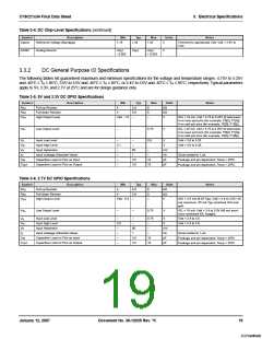
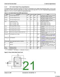
3.3.4
DC Low Power Comparator Specifications
The following table lists guaranteed maximum and minimum specifications for the voltage and temperature ranges: 4.75V to 5.25V
and -40°C ≤ TA ≤ 85°C, 3.0V to 3.6V and -40°C ≤ TA ≤ 85°C, or 2.4V to 3.0V and -40°C ≤ TA ≤ 85°C, respectively. Typical parameters
apply to 5V at 25°C and are for design guidance only.
Table 3-10. DC Low Power Comparator Specifications
Symbol
Description
Low power comparator (LPC) reference voltage range
LPC supply current
Min
Typ
Max
Vdd - 1
40
Units
Notes
V
I
0.2
–
–
V
REFLPC
10
µA
SLPC
V
LPC voltage offset
–
2.5
30
mV
OSLPC
January 12, 2007
Document No. 38-12025 Rev. *K
20
[+] Feedback

 CYPRESS [ CYPRESS ]