CY7C68013A, CY7C68014A
CY7C68015A, CY7C68016A
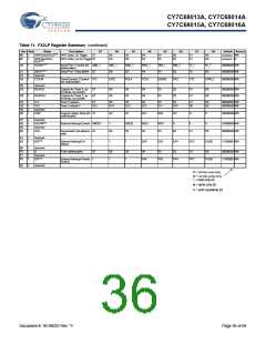
Table 11. FX2LP Register Summary (continued)
Hex Size
xxxx
Name
Description
b7
b6
b5
b4
b3
b2
b1
b0
Default Access
I²C Configuration Byte
0
DISCON
0
0
0
0
0
400KHZ
xxxxxxxx n/a
[14]
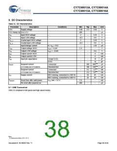
Special Function Registers (SFRs)
[13]
80
81
82
83
84
85
86
87
88
1
1
1
1
1
1
1
1
1
IOA
Port A (bit addressable)
D7
D7
A7
A15
A7
A15
0
D6
D6
A6
A14
A6
A14
0
D5
D5
A5
A13
A5
A13
0
D4
D4
A4
A12
A4
A12
0
D3
D3
A3
A11
A3
A11
0
D2
D2
A2
A10
A2
A10
0
D1
D1
A1
A9
A1
A9
0
D0
xxxxxxxx RW
00000111 RW
00000000 RW
00000000 RW
00000000 RW
00000000 RW
00000000 RW
00110000 RW
00000000 RW
SP
Stack Pointer
D0
DPL0
DPH0
Data Pointer 0 L
Data Pointer 0 H
Data Pointer 1 L
Data Pointer 1 H
Data Pointer 0/1 select
Power Control
A0
A8
[13]
DPL1
DPH1
A0
[13]
A8
[13]
DPS
SEL
IDLE
IT0
PCON
TCON
SMOD0
TF1
x
1
1
x
x
x
Timer/Counter Control
(bit addressable)
TR1
TF0
TR0
IE1
IT1
IE0
89
1
TMOD
Timer/Counter Mode
Control
GATE
CT
M1
M0
GATE
CT
M1
M0
00000000 RW
8A
8B
8C
8D
8E
8F
90
91
92
1
1
1
1
1
1
1
1
1
TL0
Timer 0 reload L
Timer 1 reload L
Timer 0 reload H
Timer 1 reload H
Clock Control
D7
D7
D15
D15
x
D6
D6
D14
D14
x
D5
D4
D3
D2
D1
D0
00000000 RW
00000000 RW
00000000 RW
00000000 RW
00000001 RW
TL1
D5
D4
D3
D2
D1
D0
TH0
D13
D13
T2M
D12
D12
T1M
D11
D11
T0M
D10
D10
MD2
D9
D8
TH1
D9
D8
[13]
CKCON
MD1
MD0
reserved
[13]
IOB
Port B (bit addressable)
D7
D6
D5
D4
D3
1
D2
0
D1
0
D0
0
xxxxxxxx RW
00001000 RW
00000000 RW
[13]
EXIF
External Interrupt Flag(s) IE5
IE4
A14
I²CINT
A13
USBNT
A12
[13]
MPAGE
Upper Addr Byte of MOVX A15
using @R0 / @R1
A11
A10
A9
A8
93
98
5
1
reserved
SCON0
Serial Port 0 Control
(bit addressable)
SM0_0
SM1_0
SM2_0
REN_0
TB8_0
RB8_0
TI_0
RI_0
00000000 RW
99
9A
9B
9C
9D
9E
9F
A0
A1
A2
A3
A8
1
1
1
1
1
1
1
1
1
1
5
1
SBUF0
Serial Port 0 Data Buffer D7
Autopointer 1 Address H A15
Autopointer 1 Address L A7
D6
D5
D4
D3
A11
A3
D2
D1
A9
A1
D0
A8
A0
00000000 RW
00000000 RW
00000000 RW
[13]
AUTOPTRH1
A14
A6
A13
A5
A12
A4
A10
A2
[13]
AUTOPTRL1
reserved
[13]
AUTOPTRH2
Autopointer 2 Address H A15
Autopointer 2 Address L A7
A14
A6
A13
A5
A12
A4
A11
A3
A10
A2
A9
A1
A8
A0
00000000 RW
00000000 RW
[13]
AUTOPTRL2
reserved
[13]
IOC
Port C (bit addressable) D7
D6
x
D5
x
D4
x
D3
x
D2
x
D1
x
D0
x
xxxxxxxx RW
[13]
INT2CLR
Interrupt 2 clear
Interrupt 4 clear
x
x
xxxxxxxx
xxxxxxxx
W
W
[13]
INT4CLR
x
x
x
x
x
x
x
reserved
IE
Interrupt Enable
(bit addressable)
EA
ES1
ET2
ES0
ET1
EX1
ET0
EX0
00000000 RW
A9
AA
1
1
reserved
[13]
EP2468STAT
Endpoint 2,4,6,8 status
flags
EP8F
EP8E
EP6F
EP6E
EP4F
EP4E
EP2F
EP2E
01011010 R
00100010 R
01100110 R
AB
AC
1
1
EP24FIFOFLGS
[13]
Endpoint 2,4 slave FIFO
status flags
0
0
EP4PF
EP8PF
EP4EF
EP8EF
EP4FF
EP8FF
0
0
EP2PF
EP6PF
EP2EF
EP6EF
EP2FF
EP6FF
EP68FIFOFLGS
[13]
Endpoint 6,8 slave FIFO
status flags
AD
AF
B0
B1
2
1
1
1
reserved
[13]
AUTOPTRSETUP
Autopointer 1&2 setup
0
0
0
0
0
APTR2INC APTR1INC APTREN
00000110 RW
xxxxxxxx RW
xxxxxxxx RW
[13]
IOD
Port D (bit addressable) D7
D6
D6
D5
D5
D4
D4
D3
D3
D2
D2
D1
D1
D0
D0
[13]
IOE
Port E
(NOT bit addressable)
D7
[13]
B2
B3
B4
B5
B6
B7
B8
1
1
1
1
1
1
1
OEA
Port A Output Enable
Port B Output Enable
Port C Output Enable
Port D Output Enable
Port E Output Enable
D7
D7
D7
D7
D7
D6
D6
D6
D6
D6
D5
D5
D5
D5
D5
D4
D4
D4
D4
D4
D3
D3
D3
D3
D3
D2
D2
D2
D2
D2
D1
D1
D1
D1
D1
D0
D0
D0
D0
D0
00000000 RW
00000000 RW
00000000 RW
00000000 RW
00000000 RW
[13]
OEB
[13]
OEC
[13]
OED
[13]
OEE
reserved
IP
Interrupt Priority (bit ad-
dressable)
1
PS1
PT2
PS0
PT1
PX1
PT0
PX0
10000000 RW
B9
BA
BB
1
1
1
reserved
[13]
EP01STAT
Endpoint 0&1 Status
0
0
0
0
0
0
0
0
0
EP1INBSY EP1OUTBSY EP0BSY
00000000 R
[13, 11]
GPIFTRIG
Endpoint 2,4,6,8 GPIF
slave FIFO Trigger
DONE
RW
EP1
EP0
10000xxx brrrrbbb
BC
BD
1
1
reserved
[13]
GPIFSGLDATH
GPIF Data H (16-bit mode D15
only)
D14
D13
D12
D11
D10
D9
D8
xxxxxxxx RW
Notes
13. SFRs not part of the standard 8051 architecture.
14. If no EEPROM is detected by the SIE then the default is 00000000.
Document #: 38-08032 Rev. *V
Page 35 of 66

 CYPRESS [ CYPRESS ]