CY7C68013A, CY7C68014A
CY7C68015A, CY7C68016A
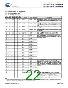
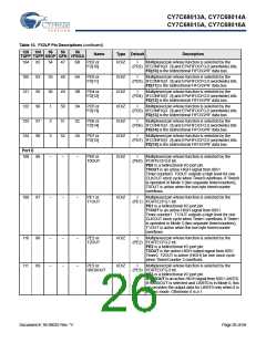
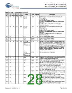
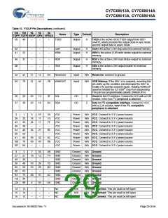
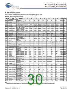
Table 10. FX2LP Pin Descriptions (continued)
128 100 56 56 56
Name
Type Default
Description
TQFP TQFP SSOP QFN VFBGA
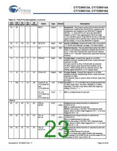
104
105
121
122
123
124
82
83
95
96
97
98
54
55
56
1
47
48
49
50
51
52
6B
6A
3B
3A
3C
2A
PD2 or
FD[10]
I/O/Z
I/O/Z
I/O/Z
I/O/Z
I/O/Z
I/O/Z
I
Multiplexed pin whose function is selected by the
(PD2) IFCONFIG[1..0] and EPxFIFOCFG.0 (wordwide) bits.
FD[10] is the bidirectional FIFO/GPIF data bus.
PD3 or
FD[11]
I
Multiplexed pin whose function is selected by the
(PD3) IFCONFIG[1..0] and EPxFIFOCFG.0 (wordwide) bits.
FD[11] is the bidirectional FIFO/GPIF data bus.
PD4 or
FD[12]
I
Multiplexed pin whose function is selected by the
(PD4) IFCONFIG[1..0] and EPxFIFOCFG.0 (wordwide) bits.
FD[12] is the bidirectional FIFO/GPIF data bus.
PD5 or
FD[13]
I
Multiplexed pin whose function is selected by the
(PD5) IFCONFIG[1..0] and EPxFIFOCFG.0 (wordwide) bits.
FD[13] is the bidirectional FIFO/GPIF data bus.
2
PD6 or
FD[14]
I
Multiplexed pin whose function is selected by the
(PD6) IFCONFIG[1..0] and EPxFIFOCFG.0 (wordwide) bits.
FD[14] is the bidirectional FIFO/GPIF data bus.
3
PD7 or
FD[15]
I
Multiplexed pin whose function is selected by the
(PD7) IFCONFIG[1..0] and EPxFIFOCFG.0 (wordwide) bits.
FD[15] is the bidirectional FIFO/GPIF data bus.
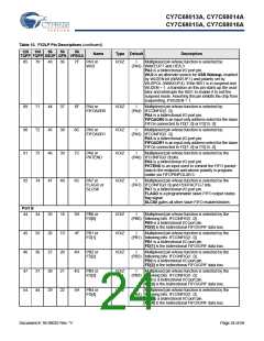
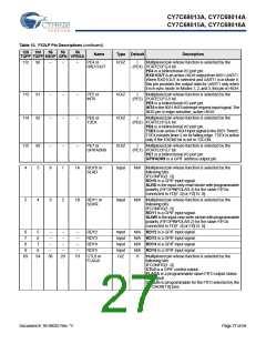
Port E
108
86
–
–
–
PE0 or
T0OUT
I/O/Z
I
Multiplexed pin whose function is selected by the
(PE0) PORTECFG.0 bit.
PE0 is a bidirectional I/O port pin.
T0OUT is an active-HIGH signal from 8051
Timer-counter0. T0OUT outputs a high level for one
CLKOUT clock cycle when Timer0 overflows. If Timer0
is operated in Mode 3 (two separate timer/counters),
T0OUT is active when the low byte timer/counter
overflows.
109
87
–
–
–
PE1 or
T1OUT
I/O/Z
I
Multiplexed pin whose function is selected by the
(PE1) PORTECFG.1 bit.
PE1 is a bidirectional I/O port pin.
T1OUT is an active-HIGH signal from 8051
Timer-counter1. T1OUT outputs a high level for one
CLKOUT clock cycle when Timer1 overflows. If Timer1
is operated in Mode 3 (two separate timer/counters),
T1OUT is active when the low byte timer/counter
overflows.
110
111
88
89
–
–
–
–
–
–
PE2 or
T2OUT
I/O/Z
I/O/Z
I
Multiplexed pin whose function is selected by the
(PE2) PORTECFG.2 bit.
PE2 is a bidirectional I/O port pin.
T2OUT is the active-HIGH output signal from 8051
Timer2. T2OUT is active (HIGH) for one clock cycle
when Timer/Counter 2 overflows.
PE3 or
RXD0OUT
I
Multiplexed pin whose function is selected by the
(PE3) PORTECFG.3 bit.
PE3 is a bidirectional I/O port pin.
RXD0OUT is an active-HIGH signal from 8051 UART0.
If RXD0OUT is selected and UART0 is in Mode 0, this
pin provides the output data for UART0 only when it is
in sync mode. Otherwise it is a 1.
Document #: 38-08032 Rev. *V
Page 26 of 66

 CYPRESS [ CYPRESS ]