CY7C68013A, CY7C68014A
CY7C68015A, CY7C68016A
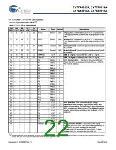
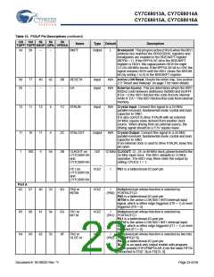
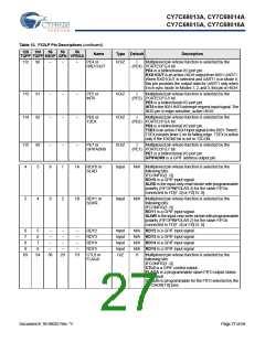
Table 10. FX2LP Pin Descriptions (continued)
128 100 56 56 56
Name
BKPT
Type Default
Description
TQFP TQFP SSOP QFN VFBGA
34
28
–
–
Output
L
Breakpoint. Thispingoesactive(HIGH)whenthe8051
address bus matches the BPADDRH/L registers and
breakpoints are enabled in the BREAKPT register
(BPEN = 1). If the BPPULSE bit in the BREAKPT
register is HIGH, this signal pulses HIGH for eight
12-/24-/48 MHz clocks. If the BPPULSE bit is LOW, the
signal remains HIGH until the 8051 clears the BREAK
bit (by writing 1 to it) in the BREAKPT register.
99
35
77
–
49
–
42
–
8B
–
RESET#
EA
Input
Input
N/A Active LOW Reset. Resets the entire chip. See section
2.9 ”Reset and Wakeup” on page 7 for more details.
N/A External Access. This pin determines where the 8051
fetches code between addresses 0x0000 and 0x3FFF.
If EA = 0 the 8051 fetches this code from its internal
RAM. IF EA = 1 the 8051 fetches this code from external
memory.
12
11
12
5
1C
XTALIN
Input
N/A Crystal Input. Connect this signal to a 24 MHz
parallel-resonant, fundamental mode crystal and load
capacitor to GND.
It is also correct to drive XTALIN with an external
24-MHz square wave derived from another clock
source. When driving from an external source, the
driving signal should be a 3.3V square wave.
11
1
10
11
5
4
2C
2B
XTALOUT
Output
O/Z
N/A Crystal Output. Connect this signal to a 24 MHz
parallel-resonant, fundamental mode crystal and load
capacitor to GND.
If an external clock is used to drive XTALIN, leave this
pin open.
100
54
CLKOUT on
CY7C68013A
and
12 MHz CLKOUT: 12-, 24- or 48 MHz clock, phase locked to the
24 MHz input clock. The 8051 defaults to 12 MHz
operation. The 8051 may three-state this output by
setting CPUCS.1 = 1.
CY7C68014A
------------------ ----------- ---------- ------------------------------------------------------------------------
PE1 on
I/O/Z
I
PE1 is a bidirectional I/O port pin.
CY7C68015A
and
CY7C68016A
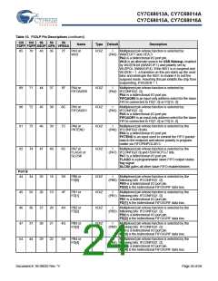
Port A
82
67
68
69
40
41
42
33
34
35
8G
6G
8F
PA0 or
INT0#
I/O/Z
I
Multiplexed pin whose function is selected by
(PA0) PORTACFG.0
PA0 is a bidirectional I/O port pin.
INT0# is the active-LOW 8051 INT0 interrupt input
signal, which is either edge triggered (IT0 = 1) or level
triggered (IT0 = 0).
83
84
PA1 or
INT1#
I/O/Z
I/O/Z
I
Multiplexed pin whose function is selected by:
(PA1) PORTACFG.1
PA1 is a bidirectional I/O port pin.
INT1# is the active-LOW 8051 INT1 interrupt input
signal, which is either edge triggered (IT1 = 1) or level
triggered (IT1 = 0).
PA2 or
I
Multiplexed pin whose function is selected by two bits:
SLOE or
(PA2) IFCONFIG[1:0].
PA2 is a bidirectional I/O port pin.
SLOE is an input-only output enable with program-
mable polarity (FIFOPINPOLAR.4) for the slave FIFOs
connected to FD[7..0] or FD[15..0].
Document #: 38-08032 Rev. *V
Page 23 of 66

 CYPRESS [ CYPRESS ]