CY7C68013A, CY7C68014A
CY7C68015A, CY7C68016A
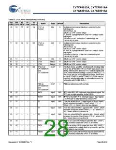
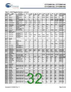
Table 10. FX2LP Pin Descriptions (continued)
128 100 56 56 56
Name
Type Default
Description
TQFP TQFP SSOP QFN VFBGA
70
55
37
30
7G
CTL1 or
FLAGB
O/Z
H
Multiplexed pin whose function is selected by the
following bits:
IFCONFIG[1..0].
CTL1 is a GPIF control output.
FLAGB is a programmable slave-FIFO output status
flag signal.
Defaults to FULL for the FIFO selected by the
FIFOADR[1:0] pins.
71
56
38
31
8H
CTL2 or
FLAGC
O/Z
H
Multiplexed pin whose function is selected by the
following bits:
IFCONFIG[1..0].
CTL2 is a GPIF control output.
FLAGC is a programmable slave-FIFO output status
flag signal.
Defaults to EMPTY for the FIFO selected by the
FIFOADR[1:0] pins.
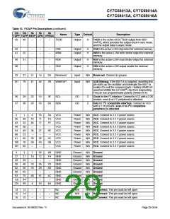
66
67
98
32
51
52
76
26
–
–
–
–
–
–
CTL3
CTL4
CTL5
O/Z
H
H
H
Z
CTL3 is a GPIF control output.
CTL4 is a GPIF control output.
CTL5 is a GPIF control output.
Output
Output
I/O/Z
–
–
–
20
13
2G
IFCLK on
CY7C68013A
and
Interface Clock, used for synchronously clocking data
into or out of the slave FIFOs. IFCLK also serves as a
timing reference for all slave FIFO control signals and
GPIF. When internal clocking is used (IFCONFIG.7 = 1)
the IFCLK pin can be configured to output 30/48 MHz
by bits IFCONFIG.5 and IFCONFIG.6. IFCLK may be
inverted, whether internally or externally sourced, by
setting the bit IFCONFIG.4 =1.
CY7C68014A
------------------ ----------- ---------- -----------------------------------------------------------------------
PE0 on
I/O/Z
I
PE0 is a bidirectional I/O port pin.
CY7C68015A
and
CY7C68016A
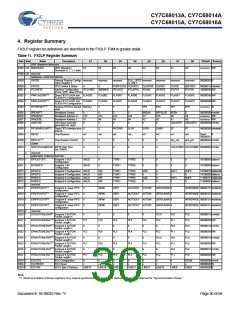
28
106
31
22
84
25
–
–
–
–
–
–
–
–
–
INT4
INT5#
T2
Input
Input
Input
N/A INT4isthe8051INT4interruptrequestinputsignal. The
INT4 pin is edge-sensitive, active HIGH.
N/A INT5# is the 8051 INT5 interrupt request input signal.
The INT5 pin is edge-sensitive, active LOW.
N/A T2 is the active-HIGH T2 input signal to 8051 Timer2,
which provides the input to Timer2 when C/T2 = 1.
When C/T2 = 0, Timer2 does not use this pin.
30
29
24
23
–
–
–
–
–
–
T1
T0
Input
Input
N/A T1 is the active-HIGH T1 signal for 8051 Timer1, which
provides the input to Timer1 when C/T1 is 1. When C/T1
is 0, Timer1 does not use this bit.
N/A T0 is the active-HIGH T0 signal for 8051 Timer0, which
provides the input to Timer0 when C/T0 is 1. When C/T0
is 0, Timer0 does not use this bit.
53
52
43
42
–
–
–
–
–
–
RXD1
TXD1
Input
N/A RXD1is an active-HIGH input signal for 8051 UART1,
which provides data to the UART in all modes.
Output
H
TXD1is an active-HIGH output pin from 8051 UART1,
which provides the output clock in sync mode, and the
output data in async mode.
51
41
–
–
–
RXD0
Input
N/A RXD0 is the active-HIGH RXD0 input to 8051 UART0,
which provides data to the UART in all modes.
Document #: 38-08032 Rev. *V
Page 28 of 66

 CYPRESS [ CYPRESS ]