CY7C68013A, CY7C68014A
CY7C68015A, CY7C68016A
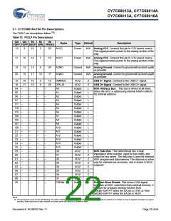
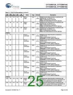
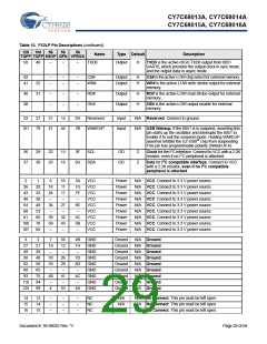
Table 10. FX2LP Pin Descriptions (continued)
128 100 56 56 56
Name
Type Default
Description
TQFP TQFP SSOP QFN VFBGA
55
56
57
45
46
47
30
31
32
23
24
25
5G
5F
6H
PB5 or
FD[5]
I/O/Z
I/O/Z
I/O/Z
I
Multiplexed pin whose function is selected by the
(PB5) following bits: IFCONFIG[1..0].
PB5 is a bidirectional I/O port pin.
FD[5] is the bidirectional FIFO/GPIF data bus.
PB6 or
FD[6]
I
Multiplexed pin whose function is selected by the
(PB6) following bits: IFCONFIG[1..0].
PB6 is a bidirectional I/O port pin.
FD[6] is the bidirectional FIFO/GPIF data bus.
PB7 or
FD[7]
I
Multiplexed pin whose function is selected by the
(PB7) following bits: IFCONFIG[1..0].
PB7 is a bidirectional I/O port pin.
FD[7] is the bidirectional FIFO/GPIF data bus.
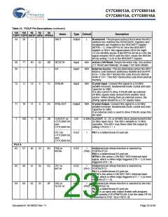
PORT C
57
72
73
74
75
76
77
78
79
–
–
–
–
–
–
–
–
–
–
–
–
–
–
–
–
–
–
–
–
–
–
–
–
PC0 or
GPIFADR0
I/O/Z
I/O/Z
I/O/Z
I/O/Z
I/O/Z
I/O/Z
I/O/Z
I/O/Z
I
Multiplexed pin whose function is selected by
(PC0) PORTCCFG.0
PC0 is a bidirectional I/O port pin.
GPIFADR0 is a GPIF address output pin.
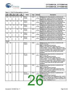
58
59
60
61
62
63
64
PC1 or
GPIFADR1
I
Multiplexed pin whose function is selected by
(PC1) PORTCCFG.1
PC1 is a bidirectional I/O port pin.
GPIFADR1 is a GPIF address output pin.
PC2 or
GPIFADR2
I
Multiplexed pin whose function is selected by
(PC2) PORTCCFG.2
PC2 is a bidirectional I/O port pin.
GPIFADR2 is a GPIF address output pin.
PC3 or
GPIFADR3
I
Multiplexed pin whose function is selected by
(PC3) PORTCCFG.3
PC3 is a bidirectional I/O port pin.
GPIFADR3 is a GPIF address output pin.
PC4 or
GPIFADR4
I
Multiplexed pin whose function is selected by
(PC4) PORTCCFG.4
PC4 is a bidirectional I/O port pin.
GPIFADR4 is a GPIF address output pin.
PC5 or
GPIFADR5
I
Multiplexed pin whose function is selected by
(PC5) PORTCCFG.5
PC5 is a bidirectional I/O port pin.
GPIFADR5 is a GPIF address output pin.
PC6 or
GPIFADR6
I
Multiplexed pin whose function is selected by
(PC6) PORTCCFG.6
PC6 is a bidirectional I/O port pin.
GPIFADR6 is a GPIF address output pin.
PC7 or
I
Multiplexed pin whose function is selected by
GPIFADR7
(PC7) PORTCCFG.7
PC7 is a bidirectional I/O port pin.
GPIFADR7 is a GPIF address output pin.
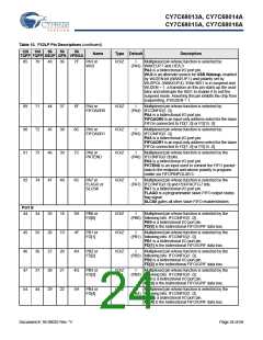
PORT D
102
80
52
53
45
46
8A
7A
PD0 or
FD[8]
I/O/Z
I/O/Z
I
Multiplexed pin whose function is selected by the
(PD0) IFCONFIG[1..0] and EPxFIFOCFG.0 (wordwide) bits.
FD[8] is the bidirectional FIFO/GPIF data bus.
103
81
PD1 or
FD[9]
I
Multiplexed pin whose function is selected by the
(PD1) IFCONFIG[1..0] and EPxFIFOCFG.0 (wordwide) bits.
FD[9] is the bidirectional FIFO/GPIF data bus.
Document #: 38-08032 Rev. *V
Page 25 of 66

 CYPRESS [ CYPRESS ]