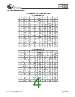
CY7C1360B
CY7C1362B
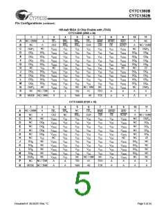
CY7C1360B–Pin Definitions (continued)
TQFP
3-Chip
Enable
TQFP
2-Chip
Enable
Name
VSSQ
BGA
fBGA
I/O
Description
5,10,21,26, 5,10,21,26,
55,60,71, 55,60,71,
-
-
I/O Ground Ground for the I/O circuitry.
76
76
VDDQ
4,11,20,27, 4,11,20,27, A1,F1,J1, C3,C9,D3,
I/O Power Power supply for the I/O circuitry.
54,61,70, 54,61,70,
M1,U1, D9,E3,E9,F
A7,F7,J7, 3,F9,G3,
Supply
77
77
M7,U7
G9,J3,J9,
K3,K9,L3,
L9,M3,M9,
N3,N9
MODE
31
31
R3
R1
Input-
Static
Selects Burst Order. When tied to GND selects
linear burst sequence. When tied to VDD or left
floating selects interleaved burst sequence. This is
a strap pin and should remain static during device
operation. Mode pin has an internal pull-up.
TDO
TDI
-
-
-
-
-
-
-
-
U5
U3
U2
U4
P7
P5
R5
R7
JTAG serial Serial data-out to the JTAG circuit. Delivers data
output
on the negative edge of TCK. If the JTAG feature is
Synchronous not being utilized, this pin should be disconnected.
This pin is not available on TQFP packages.
JTAG serial Serial data-In to the JTAG circuit. Sampledonthe
input
rising edge of TCK. If the JTAG feature is not being
Synchronous utilized, this pin can be disconnected or connected
to VDD. This pin is not available on TQFP packages.
TMS
TCK
NC
JTAG serial Serial data-In to the JTAG circuit. Sampledonthe
input
rising edge of TCK. If the JTAG feature is not being
Synchronous utilized, this pin can be disconnected or connected
to VDD. This pin is not available on TQFP packages.
JTAG-Clock Clock input to the JTAG circuitry. If the JTAG
feature is not being utilized, this pin must be
connected to VSS. This pin is not available on TQFP
packages.
14,16,66, 14,16,38,
B1,C1, A11,B1,C2,
-
No Connects. Not internally connected to the die
42,39,38 39,42,43, R1,T1,T2, C10,H1,H3,
66,
J3,D4,
H9,H10,
L4,5J,5R, N2,N5,N7,
6T,6U, N10,P1,A1,
B7,C7, B11,P2,R2,
R7
N6
Document #: 38-05291 Rev. *C
Page 8 of 34

 CYPRESS [ CYPRESS ]