CY7C1360B
CY7C1362B
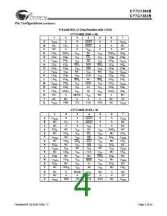
CY7C1360B–Pin Definitions
TQFP
3-Chip
Enable
TQFP
2-Chip
Enable
Name
BGA
fBGA
I/O
Description
Address Inputs used to select one of the 256K
A0, A1, A
37,36,32, 37,36,32,
33,34,35, 33,34,35,
43,44,45, 44,45,46,
46,47,48, 47,48,49,
P4,N4, R6,P6,A2,
Input-
A2,C2,
A10,B2, Synchronous address locations. Sampled at the rising edge of
R2,3A, B10,P3,P4,
B3,C3, P8,P9,P10,
the CLK if
or
is active LOW, and CE ,
ADSP ADSC
CE2, and CE3[2]are sampled active. A1, A0 are fe1d
49,50,81, 50,81,82, T3,T4,A5, P11,R3,R4,
82,99,100 92,99,100 B5,C5, R8,R9,R10,
to the two-bit counter.
.
T5,A6,B6,
C6,R6
R11
93,94,95, 93,94,95,
L5,G5,
G3,L3
B5,A5,A4,
B4
Input-
Byte Write Select Inputs, active LOW. Qualified
with BWE to conduct Byte Writes to the SRAM.
Sampled on the rising edge of CLK.
BWA,BWB
BWC,BWD
96
96
Synchronous
H4
B7
Input-
Global Write Enable Input, active LOW. When
88
88
GW
Synchronous asserted LOW on the rising edge of CLK, a global
Write is conducted (ALL bytes are written,
regardless of the values on BWX and BWE).
87
89
87
89
M4
K4
A7
B6
Input-
Byte Write Enable Input, active LOW. Sampled
BWE
CLK
Synchronous on the rising edge of CLK. This signal must be as-
serted LOW to conduct a Byte Write.
Input-
Clock
Clock Input. Used to capture all synchronous
inputs to the device. Also used to increment the
burst counter when ADV is asserted LOW, during a
burst operation.
98
98
E4
A3
Input-
Chip Enable 1 Input, active LOW. Sampled on the
CE1
CE2
Synchronous rising edge of CLK. Used in conjunction with CE2
and CE3[2] to select/deselect the device. ADSP is
ignored if CE1 is HIGH.
97
92
97
-
B2
-
B3
A6
Input-
Chip Enable 2 Input, active HIGH. Sampled on
Synchronous the rising edge of CLK. Used in conjunction with
CE1 and CE3[2] to select/deselect the device.
Input-
Chip Enable 3 Input, active LOW. Sampled on the
[2]
CE3
Synchronous rising edge of CLK. Used in conjunction with CE1
andCE2 toselect/deselectthedevice. Notavailable
for AJ package version.
Not connected for BGA.
Where referenced, CE3[2] is assumed active
throughout this document for BGA.
86
83
86
83
F4
B8
A9
Input-
Output Enable, asynchronous input, active
OE
Asynchro- LOW. Controls the direction of the I/O pins. When
nous
LOW, the I/O pins behave as outputs. When
deassertedHIGH, I/Opinsarethree-stated, andact
as input data pins. OE is masked during the first
clock of a read cycle when emerging from a
deselected state.
G4
Input-
Advance Input signal, sampled on the rising
ADV
Synchronous edge of CLK, active LOW. When asserted, it
automatically increments the address in a burst
cycle.
Document #: 38-05291 Rev. *C
Page 6 of 34

 CYPRESS [ CYPRESS ]