CY7C1360B
CY7C1362B
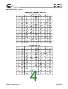
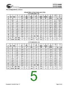
CY7C1360B–Pin Definitions (continued)
TQFP
3-Chip
Enable
TQFP
2-Chip
Enable
Name
ADSP
BGA
fBGA
I/O
Description
Address Strobe from Processor, sampled on
84
84
A4
B9
Input-
Synchronous the rising edge of CLK, active LOW. When
asserted LOW, addresses presented to the device
are captured in the address registers. A1, A0 are
also loaded into the burst counter. When ADSP and
ADSC are both asserted, only ADSP is recognized.
ASDP is ignored when CE1 is deasserted HIGH.
85
64
B4
T7
A8
Input-
AddressStrobefromController, sampledonthe
85
64
ADSC
ZZ
Synchronous rising edge of CLK, active LOW. When asserted
LOW, addresses presented to the device are
captured in the address registers. A1, A0 are also
loaded into the burst counter. When ADSP and
ADSC are both asserted, only ADSP is recognized.
H11
Input-
ZZ “Sleep” Input, active HIGH. When asserted
Asynchro- HIGH places the device in a non-time-critical
nous
“sleep” condition with data integrity preserved. For
normal operation, this pin has to be LOW or left
floating. ZZ pin has an internal pull-down.
52,53,56, 52,53,56,
57,58,59, 57,58,59,
62,63,68, 62,63,68,
69,72,73, 69,72,73,
74,75,78, 74,75,78,
K6,L6,
M6,N6,
K7,L7,
N7,P7,
E6,F6,
M11,L11,
I/O-
Bidirectional Data I/O lines. As inputs, they feed
DQs,
K11,J11, Synchronous into an on-chip data register that is triggered by the
DQPs
J10,K10,
L10,M10,
D10,E10,
F10,G10,
D11,E11,
F11,G11,
D1,E1,F1,
risingedge of CLK. As outputs, they deliver the data
contained in the memory location specified by the
addresses presented during the previous
clock rise
79,2,3,6,7, 79,2,3,6,7, G6,H6,
8,9,12,13,1 8,9,12,13,1 D7,E7,
of the read cycle. The direction of the pins is
controlled by OE. When OE is asserted LOW, the
pins behave as outputs. When HIGH, DQs and
DQPX are placed in a three-state condition.
8,19,22,
8,19,22,
G7,H7,
D1,E1,
23,24,25, 23,24,25,
28,29,51, 28,29,51,
G1,H1, G1,D2,E2,
80,1,30
80,1,30
E2,F2,
F2,G2,J1,
G2,H2, K1,L1,M1,
K1,L1,
N1,P1,
J2,K2,L2,
M2,N11,
K2,L2, C11,C1,N1
M2,N2,
P6,D6,
D2,P2
VDD
15,41,65, 15,41,65, J2,C4,J4, D4,D8,E4, PowerSupply Power supply inputs to the core of the device.
91
91
R4,J6
E8,F4,F8,
G4,G8,H4,
H8,J4,J8,
K4,K8,L4,
L8,M4,M8
VSS
17,40,67, 17,40,67,
90 90
D3,E3, C4,C5,C6,
F3,H3, C7,C8,D5,
K3,M3, D6,D7,E5,
Ground
Ground for the core of the device.
N3,P3,
D5,E5,
E6,E7,F5,
F6,F7,G5,
F5,H5, G6,G7,H2,
K5,M5, H5,H6,H7,J
N5,P5
5,J6,J7,
K5,K6,K7,
L5,L6,L7,
M5,M6,M7,
N4,N8
Document #: 38-05291 Rev. *C
Page 7 of 34

 CYPRESS [ CYPRESS ]