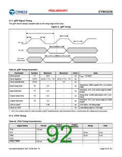
PRELIMINARY
CYW43438
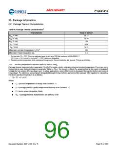
23. Package Information
23.1 Package Thermal Characteristics
Table 46. Package Thermal Characteristics1
Characteristic
Value in Still Air
JA (°C/W)
JB (°C/W)
JC (°C/W)
54.75
15.38
7.16
0.04
14.21
125
(°C/W)
JT
(°C/W)
JB
2
Maximum Junction Temperature T (°C)
j
Maximum Power Dissipation (W)
1.2
1. No heat sink, TA = 70°C. This is an estimate based on a 4-layer PCB that conforms to EIA/JESD51–7
(101.6 mm x 114.3 mm x 1.6 mm) and P = 1.2W continuous dissipation.
2. Absolute junction temperature limits maintained through active thermal monitoring and dynamic TX duty cycle limiting.
23.1.1 Junction Temperature Estimation and PSI Versus Thetajc
Package thermal characterization parameter PSI-JT ( ) yields a better estimation of actual junction temperature (T ) versus using
JT
J
the junction-to-case thermal resistance parameter Theta-J (JC). The reason for this is JC assumes that all the power is dissipated
C
through the top surface of the package case. In actual applications, some of the power is dissipated through the bottom and sides of
the package. takes into account power dissipated through the top, bottom, and sides of the package. The equation for calculating
JT
the device junction temperature is as follows:
TJ = TT + P JT
Where:
■
T = junction temperature at steady-state condition, °C
J
■
T = package case top center temperature at steady-state condition, °C
T
■
■
P = device power dissipation, Watts
= package thermal characteristics (no airflow), °C/W
JT
Document Number: 002-14796 Rev. *K
Page 96 of 101

 CYPRESS [ CYPRESS ]