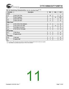
CY7C1359A/GVT71256T18
Performing a TAP Reset
IEEE 1149.1 Serial Boundary Scan (JTAG)
The TAP circuitry does not have a Reset pin (TRST, which is
optional in the IEEE 1149.1 specification). A RESET can be
performed for the TAP controller by forcing TMS HIGH (VCC)
for five rising edges of TCK and pre-loads the instruction reg-
ister with the IDCODE command. This type of reset does not
affect the operation of the system logic. The reset affects test
logic only.
Overview
This device incorporates a serial boundary scan access port
(TAP). This port is designed to operate in a manner consistent
with IEEE Standard 1149.1-1990 (commonly referred to as
JTAG), but does not implement all of the functions required for
IEEE 1149.1 compliance. Certain functions have been modi-
fied or eliminated because their implementation places extra
delays in the critical speed path of the device. Nevertheless,
the device supports the standard TAP controller architecture
(the TAP controller is the state machine that controls the TAP’s
operation) and can be expected to function in a manner that
does not conflict with the operation of devices with IEEE Stan-
dard 1149.1 compliant TAPs. The TAP operates using
LVTTL/LVCMOS logic level signaling.
At power-up, the TAP is reset internally to ensure that TDO is
in a High-Z state.
Test Access Port (TAP) Registers
Overview
The various TAP registers are selected (one at a time) via the
sequences of ones and zeros input to the TMS pin as the TCK
is strobed. Each of the TAP’s registers are serial shift registers
that capture serial input data on the rising edge of TCK and
push serial data out on subsequent falling edge of TCK. When
a register is selected, it is connected between the TDI and
TDO pins.
Disabling the JTAG Feature
It is possible to use this device without using the JTAG feature.
To disable the TAP controller without interfering with normal
operation of the device, TCK should be tied LOW (VSS) to
prevent clocking the device. TDI and TMS are internally pulled
up and may be unconnected. They may alternately be pulled
up to VCC through a resistor. TDO should be left unconnected.
Upon power-up the device will come up in a reset state which
will not interfere with the operation of the device.
Instruction Register
The instruction register holds the instructions that are execut-
ed by the TAP controller when it is moved into the run test/idle
or the various data register states. The instructions are three
bits long. The register can be loaded when it is placed between
the TDI and TDO pins. The parallel outputs of the instruction
register are automatically preloaded with the IDCODE instruc-
tion upon power-up or whenever the controller is placed in the
test-logic reset state. When the TAP controller is in the Cap-
ture-IR state, the two least significant bits of the serial instruc-
tion register are loaded with a binary “01” pattern to allow for
fault isolation of the board-level serial test data path.
Test Access Port (TAP)
TCK - Test Clock (INPUT)
Clocks all TAP events. All inputs are captured on the rising
edge of TCK and all outputs propagate from the falling edge
of TCK.
TMS - Test Mode Select (INPUT)
The TMS input is sampled on the rising edge of TCK. This is
the command input for the TAP controller state machine. It is
allowable to leave this pin unconnected if the TAP is not used.
The pin is pulled up internally, resulting in a logic HIGH level.
Bypass Register
The bypass register is a single-bit register that can be placed
between TDI and TDO. It allows serial test data to be passed
through the device TAP to another device in the scan chain
with minimum delay. The bypass register is set LOW (VSS
when the BYPASS instruction is executed.
)
TDI - Test Data In (INPUT)
The TDI input is sampled on the rising edge of TCK. This is the
input side of the serial registers placed between TDI and TDO.
The register placed between TDI and TDO is determined by
the state of the TAP controller state machine and the instruc-
tion that is currently loaded in the TAP instruction register (re-
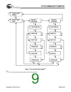
fer to Figure 1, TAP Controller State Diagram). It is allowable
to leave this pin unconnected if it is not used in an application.
The pin is pulled up internally, resulting in a logic HIGH level.
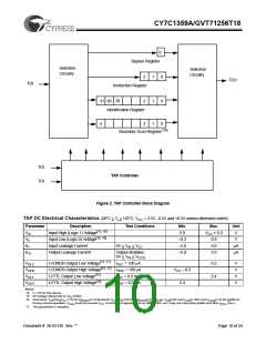
TDI is connected to the most significant bit (MSB) of any reg-
ister. (See Figure 2.)
Boundary Scan Register
The Boundary scan register is connected to all the input and
bidirectional I/O pins (not counting the TAP pins) on the device.
This also includes a number of NC pins that are reserved for
future needs. There are a total of 70 bits for a x36 device and
51 bits for a x18 device. The boundary scan register, under the
control of the TAP controller, is loaded with the contents of the
device I/O ring when the controller is in Capture-DR state and
then is placed between the TDI and TDO pins when the con-
troller is moved to Shift-DR state. The EXTEST, SAMPLE/
PRELOAD and SAMPLE-Z instructions can be used to cap-
ture the contents of the I/O ring.
TDO - Test Data Out (OUTPUT)
The TDO output pin is used to serially clock data-out from the
registers. The output that is active depending on the state of
the TAP state machine (refer to Figure 1, TAP Controller State
Diagram). Output changes in response to the falling edge of
TCK. This is the output side of the serial registers placed be-
tween TDI and TDO. TDO is connected to the least significant
bit (LSB) of any register. (See Figure 2.)
The Boundary Scan Order table describes the order in which
the bits are connected. The first column defines the bit’s posi-
tion in the boundary scan register. The MSB of the register is
connected to TDI, and LSB is connected to TDO. The second
column is the signal name and the third column is the bump
number. The third column is the TQFP pin number and the
fourth column is the BGA bump number.
Document #: 38-05120 Rev. **
Page 7 of 24

 CYPRESS [ CYPRESS ]