CY7C1359A/GVT71256T18
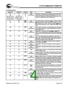
Pin Descriptions (continued)
BGA Pins
TQFP Pins
Name
Type
Description
6P
51
MOE
Input
Match Output Enable: This active LOW asynchronous input
enables the MATCH output drivers.
7P, 6N, 6L, 7K, 58,59, 62, 63, 68, DQ1–
Input/
Output
Data Inputs/Outputs: Input data must meet setup and hold
times around the rising edge of CLK.
6H, 7G, 6F, 7E, 69, 72, 73, 74, 8,
6D, 1D, 2E, 2G, 9, 12, 13, 18, 19,
DQ18
1H, 2K, 1L, 2M,
22, 23, 24
1N, 2P
5U
42
TDO
Output
Input
IEEE 1149.1 test output. LVTTL-level output.
IEEE 1149.1 test inputs. LVTTL-level inputs.
2U
3U
4U
38
39
43
TMS
TDI
TCK
4C, 2J, 4J, 6J, 4R
15, 41,65, 91
VCC
VSS
Supply
Ground
Power Supply: +3.3V –5% and +10%
3D, 5D, 3E, 5E, 5, 10, 17, 21, 26,
3F, 5F, 5G, 3H, 40,55, 60, 67, 71,
Ground: GND
5H, 3K, 5K, 3L,
3M, 5M, 3N, 5N,
3P, 5P
76, 90
1A,7A,1F,7F,1J, 4, 11, 20, 27, 54,
VCCQ
I/O Supply
-
Output Buffer Supply: +2.5V (from 2.375V to VCC)
7J, 1M, 7M, 1U,
7U
61, 70, 77
1B, 7B, 1C, 7C,
1-3, 6, 7, 14, 16,
NC
No Connect: These signals are not internally connected.
2D, 4D, 7D, 1E, 25, 28-30, 56, 57,
6E, 2F, 1G, 6G, 66,75, 78, 79, 95,
2H, 7H, 3J, 5J,
1K, 6K, 2L, 4L,
7L, 2N, 1P, 1R,
5R, 7R, 1T, 4T, 6U
96
Burst Address Table (MODE = GND)
Burst Address Table (MODE = NC/V
)
CC
First
Address
(external)
Second
Address
(internal)
Third
Address
(internal)
Fourth
Address
(internal)
First
Address
(external)
Second
Address
(internal)
Third
Address
(internal)
Fourth
Address
(internal)
A...A00
A...A01
A...A10
A...A11
A...A01
A...A10
A...A11
A...A00
A...A10
A...A11
A...A00
A...A01
A...A11
A...A00
A...A01
A...A10
A...A00
A...A01
A...A10
A...A11
A...A01
A...A00
A...A11
A...A10
A...A10
A...A11
A...A00
A...A01
A...A11
A...A10
A...A01
A...A00
Partial Truth Table for MATCH[2, 3, 4, 5, 6]
Operation
READ Cycle
E
L
WE
H
L
DEN
MOE
OE
MATCH
DQ
Q
X
L
X
X
X
L
L
H
H
H
X
X
-
WRITE Cycle
L
-
-
D
Fill WRITE Cycle
L
L
H
L
High-Z
D
COMPARE Cycle
L
H
X
Output
H
Deselected Cycle (MATCH Out)
H
H
X
X
L
High-Z
High-Z
Deselected Cycle
X
H
High-Z
Notes:
2. X means “don’t care.” H means logic HIGH. L means logic LOW. It is assumed in this table that ADSP is HIGH and ADSC is LOW.
3. E=L is defined as CE=LOW and CE2=LOW and CE2=HIGH. E =H is defined as CE=HIGH or CE2=HIGH or CE2=LOW. WE is defined as [BWE + WEL*WEH]*GW.
4. All inputs except OE and MOE must meet setup and hold times around the rising edge (LOW to HIGH) of CLK.
5. For a write operation following a read operation, OE must be HIGH before the input data required setup time plus High-Z time for OE and staying HIGH throughout
the input data hold time.
6. This device contains circuitry that will ensure the outputs will be in High-Z during power-up.
Document #: 38-05120 Rev. **
Page 5 of 24

 CYPRESS [ CYPRESS ]