RF Quadrature Transceiver / RF Quadrature Receiver
CMX991/CMX992
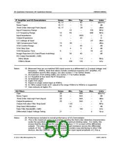
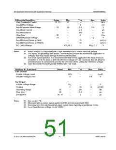
Differential Amplifiers
Notes
Min.
Typ.
Max.
Units
Gain Bandwidth Product
30, 33
11
14
–
MHz
Input Offset Voltage
Input Common Mode Range
Input Bias Current
–
1
1.6
0.4
160
6
–
mV
V
32
1.0
2.5
–
–
µA
Input Resistance
–
–
kΩ
Slew Rate
30
31
–
–
V/µs
V
Differential Input Voltage
Input Referred Noise at 1kHz
Input Referred Noise at 450kHz
DC Output Range
–
–
1.2
–
–
15
10
–
–
–
nV/Hz
nV/Hz
V
AVss+0.1
AVDD-0.1
Notes:
30. With a load of 1kΩ in parallel with 100pF referenced to a virtual earth not ground.
31. The inputs are protected with diodes. These diodes prevent the inadvertent application of
voltages that may cause damage to the input transistors.
32. For small signal operation. It is recommended that for this application the input levels be
restricted to +/-0.4V about a defined reference voltage of 1.6V (nominal); this will allow for
some tolerance in components and for the precision of the setting the reference voltage.
33. Gain Bandwidth Product typically 40MHz with 15pF load.
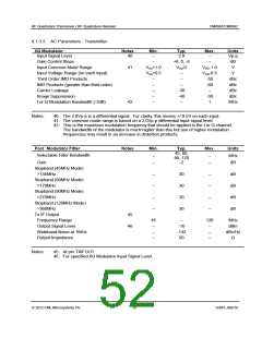
Auxiliary Rx Functions
Notes
Min.
Typ.
Max.
Units
LNA Control
Enable Voltage Level
Disable Voltage Level
80%
0
–
–
–
VDDIO
V
0.4
SLI Output
Output Voltage Range
Scaling
Vref.
5
–
10
50
0.2
1
–
15
–
V
mV/dB
dB
Operating Range
Rise time
35
36
–
–
–
µs
Decay time
36, 37
–
–
µs
Notes:
35. See section 7.8.
36. Measured with a pulsed signal applied to IFIN and terminated with 50Ω.
37. Recovery from SLI saturated (high input signal) takes typically an additional 500ns.
38. Vref is the reference voltage on pin VBIAS.
2012 CML Microsystems Plc
51
D/991_992/18

 CMLMICRO [ CML MICROCIRCUITS ]