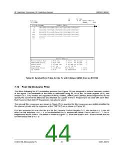
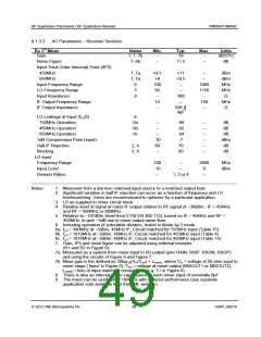
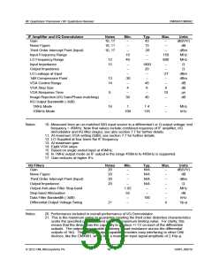
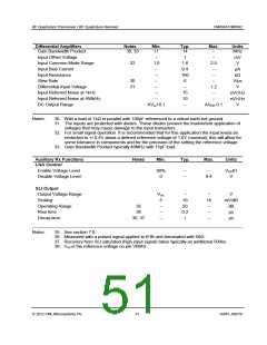
RF Quadrature Transceiver / RF Quadrature Receiver
CMX991/CMX992
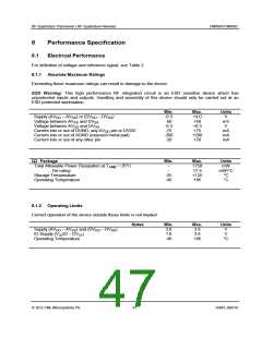
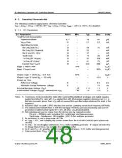
8.1.3 Operating Characteristics
The following conditions apply unless otherwise specified:
V
DD
= AV = DV = 3.0V to 3.6V; V = AV = DV
T
= -40°C to +85°C, SLI disabled.
DD
DD
SS
SS
SS, AMB
8.1.3.1 DC Parameters
DC Parameters
Notes
Min.
Typ.
Max.
Units
Total Current Consumption
Powersave Mode
A, F
C
–
–
10
60
µA
V
BIAS
Only
2.1
2.6
mA
Operating Currents
Rx Only (with SLI)
Rx Only (SLI Disabled)
Rx IF and PLL Only
Synth Only
J
D
–
–
58
52
37
14
82
61
0.3
–
75
–
mA
mA
D
H
–
–
mA
D
–
20
108
76
600
–
mA
Tx Only (RF Output)
Tx Only (IF Output)
Current from VDDIO
Logic ‘1’ Input Level
Logic ‘0’ Input Level
G
G
B
–
mA
–
mA
–
µA
70%
–
VDDIO
VDDIO
–
30%
Output Logic ‘1’ Level (l = 0.6 mA)
80%
–
–
–
VDDIO
V
OH
Output Logic ‘0’ Level (l = -1.0 mA)
–
+0.4
OL
Power-up Time
Reference Voltage
E
E
–
–
–
–
0.5
10
ms
µs
All Blocks Except Reference Voltage
Internal Bandgap Voltage (V
)
1.06
1.45
1.13
1.6
1.2
1.75
V
V
BG
External Bias Voltage (V
) – derived from V
BIAS
BG
Notes: A. Powersave mode includes the state after General Reset with all analogue and digital supplies
applied and also the case with V applied but with all analogue supplies disconnected (i.e. in
DD
this later scenario, power from V will not exceed the specified value whatever the state of the
DD
registers).
B. Assumes 30pF on each C-BUS interface line and an operating serial clock frequency of 5MHz.
C. The stated current drawn here is with the bandgap reference and accompanying bias current
generators enabled only (register $11, b7), all other circuitry is disabled.
D. Not including any current drawn from the device pins by external circuitry:
Rx only – All Rx circuitry including SLI , synthesiser and bias generator.
Synth only – Synthesiser, NR Amplifier, VCO Buffer and bias generator.
E. As measured from the rising edge of CSN.
F. At T
= 25ºC, not including any current drawn from the CMX991/CMX992 pins by external
AMB
circuitry.
G. Tx only – Tx circuitry plus synthesiser, VCO, buffer and bias generator. IF output excludes the
Tx Image Reject Mixer, but includes the IF Output buffer.
H. Rx IF and PLL – IF amplifier and I/Q mixers plus synthesiser, VCO, buffer and bias generator
J. Total current from AV
DV
and VDDIO.
DD
DD
,
2012 CML Microsystems Plc
48
D/991_992/18

 CMLMICRO [ CML MICROCIRCUITS ]