RF Quadrature Transceiver / RF Quadrature Receiver
CMX991/CMX992
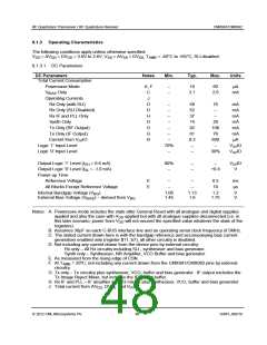
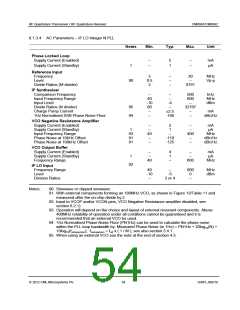
8.1.3.4 AC Parameters – IF LO Integer N PLL
Notes
Min.
Typ.
Max.
Unit
Phase Locked Loop
Supply Current (Enabled)
–
–
5
1
–
–
mA
µA
Supply Current (Standby)
1
Reference Input
Frequency
Level
5
0.5
2
–
–
–
30
–
8191
MHz
Vp-p
90
Divide Ratios (M divider)
IF Synthesiser
Comparison Frequency
Input Frequency Range
Input Level
Divide Ratios (N divider)
Charge Pump Current
1Hz Normalised SSB Phase Noise Floor
–
40
-10
80
–
–
–
-4
–
2.5
-198
500
600
–
32767
–
kHz
MHz
dBm
95
94
mA
dBc/Hz
–
–
VCO Negative Resistance Amplifier
Supply Current (Enabled)
Supply Current (Standby)
–
–
2
1
–
–
mA
µA
1
Input Frequency Range
Phase Noise at 10kHz Offset
Phase Noise at 100kHz Offset
93
91
91
40
–
–
–
-110
-125
400
–
–
MHz
dBc/Hz
dBc/Hz
VCO Output Buffer
Supply Current (Enabled)
Supply Current (Standby)
Frequency Range
–
–
40
4
1
–
–
–
600
mA
µA
MHz
1
92
IF LO Input
Frequency Range
Level
40
-10
–
–
-5
2 or 4
600
0
–
MHz
dBm
Division Ratios
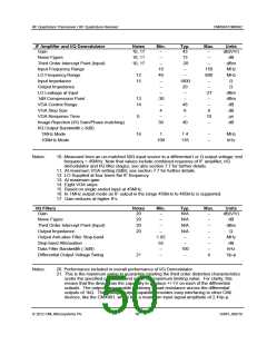
Notes:
90. Sinewave or clipped sinewave.
91. With external components forming an 180MHz VCO, as shown in Figure 13/Table 11 and
measured after the on-chip divide by 2.
92. Input to VCOP and/or VCON pins, VCO Negative Resistance amplifier disabled, see
section 6.2.1).
93. Operation will depend on the choice and layout of external resonant components. Above
400MHz reliability of operation under all conditions cannot be guaranteed and it is
recommended that an external VCO be used.
94. 1Hz Normalised Phase Noise Floor (PN1Hz) can be used to calculate the phase noise
within the PLL loop bandwidth by: Measured Phase Noise (in 1Hz) = PN1Hz + 20log10(N) +
10log10(fcomparison); fcomparison = fref x ( 1 / M ), see also section 5.4.1.
95. When using an external VCO see the note at the end of section 4.5.
2012 CML Microsystems Plc
54
D/991_992/18

 CMLMICRO [ CML MICROCIRCUITS ]