RF Quadrature Transceiver / RF Quadrature Receiver
CMX991/CMX992
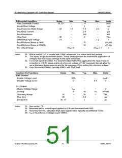
8
Performance Specification
8.1
Electrical Performance
For definition of voltage and reference signal, see Table 2.
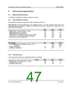
8.1.1 Absolute Maximum Ratings
Exceeding these maximum ratings can result in damage to the device.
ESD Warning: This high performance RF integrated circuit is an ESD sensitive device which has
unprotected inputs and outputs. Handling and assembly of this device should only be carried out at an
ESD protected workstation.
Min.
-0.3
-50
-0.3
-75
Max.
+4.0
+50
+0.3
+75
Units
V
mV
V
mA
mA
mA
Supply (AV – AV ) or (DV – DV )
SS
DD
SS
DD
Voltage between AV and DV
SS
SS
Voltage between AV and DV
DD
DD
Current into or out of DGND, any AV pin or DVDD
DD
Current into or out of AGND (exposed metal pad)
Current into or out of any other pin
-200
-20
+200
+20
Q3 Package
Total Allowable Power Dissipation at T
... De-rating
Storage Temperature
Operating Temperature
Min.
–
–
-55
-40
Max.
1750
17.5
+125
+85
Units
mW
mW/°C
°C
= 25°C
AMB
°C
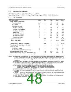
8.1.2 Operating Limits
Correct operation of the device outside these limits is not implied.
Notes
Min.
3.0
Max.
3.6
Units
V
Supply (AV – AV ) and (DV – DV )
SS
DD
SS
DD
IO Supply (VDDIO – DVSS)
1.6
3.6
V
Operating Temperature
-40
+85
°C
2012 CML Microsystems Plc
47
D/991_992/18

 CMLMICRO [ CML MICROCIRCUITS ]