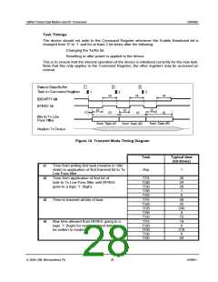
GMSK Packet Data Modem and RF Transceiver
CMX990
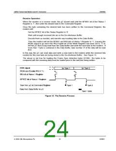
Receive Operation
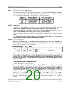
When the modem is in receive mode, the µC should wait until the BFREE bit of the Status 1
Register is ‘1’, then write the desired task to the Command Register.
Once the byte containing the desired task has been written to the Command Register, the
modem will:
Set the BFREE bit of the Status Register to ‘0’.
Wait until enough received bits are in the De-interleave Buffer.
Decode them as needed, and transfer any resulting data to the Data Buffer.
Then the modem will set the BFREE and IRQ bits of Status 1 Register to ‘1’, (causing the
IRQN output to go low if the IRQ Enable bit of the Mode Register has been set to ‘1’) to
tell the µC that it may read from the Data Buffer and write the next task to the modem. If
more than 1 byte is contained in the Data Buffer, byte number ‘0’ of the data will be read
first.
In this way the µC can read data and write a new task to the modem while the received bits
needed for this new task are being stored in the De-interleave Buffer. See Figure 13.
The above is not true for loading the Frame Sync detection bytes (LFSB): the bytes to be
compared with the incoming data must be loaded prior to the task bits being written.
Figure 13 The Receive Process
ã 2004 CML Microsystems Plc
24
D/990/1

 CMLMICRO [ CML MICROCIRCUITS ]