GMSK Packet Data Modem and RF Transceiver
CMX990
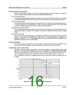
5.1.4
Programmer’s View of the Modem
The modem appears to the programmer as a series of 8-bit read and write registers, individual
registers being selected by the A0 to A5 address pins. Most of the baseband control for
formatting or decoding the data is controlled by the following registers:
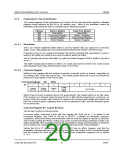
Address
$00
Write to Modem
Data Buffer
Read from Modem
Data Buffer
$01
$02
$03
Command Register
Control Register
Mode Register
Status 1 Register
Data Quality Register
Status 2 Register
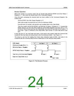
5.1.4.1 Data Buffer
This is an 18-byte read/write buffer which is used to transfer data (as opposed to command,
status, mode, data quality and control information) between the modem and the host µC.
It appears to the µC as a single 8-bit register; the modem ensuring that sequential µC reads or
writes to the buffer are routed to the correct locations within the buffer.
The µC should only access this buffer 2 µs after the Status Register BFREE (Buffer Free) bit is
set to ‘1’.
The buffer should only be written to while in Tx mode and read from while in Rx mode (except
when loading Frame Sync detection bytes while in Rx mode).
5.1.4.2 Command Register
Writing to this register tells the modem to perform a specific action or actions, depending on
the setting of the TASK and acquire bits. The enable packet detect bit is used to indicate the
presence of data signals in the receive path.
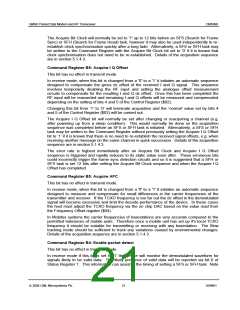
Command Register
$01
Write
7
6
5
4
3
2
1
0
Bit:
Enable
packet
detect
Acquire
Bit Clock
Acquire
I Q Offset
Acquire
AFC
Task Control
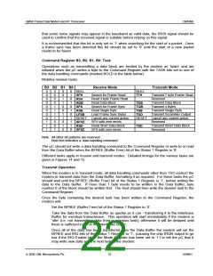
When it has no action to perform (but is not ‘powersaved’), the modem will be in an ‘idle’ state.
If the modem is in transmit mode the input to the Tx filter will be connected to a mid level. In
receive mode the modem will continue to measure the received data quality and extract bits
from the received signal, supplying them to the de-interleave buffer, but will otherwise ignore
the received data.
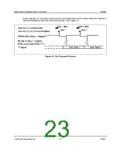
Command Register B7: Acquire Bit Clock
This bit has no effect in transmit mode.
In receive mode, whenever a byte with the Acquire Bit Clock set to ‘1’ is written to the
Command Register, and TASK is not set to RESET, it initiates an automatic sequence
designed to achieve bit timing synchronisation with the received signal as quickly as possible.
This involves setting the Phase Locked Loop of the received bit timing extraction circuits to its
widest bandwidth, then gradually reducing the bandwidth as timing synchronisation is achieved,
until it reaches the 'normal' value set by the PLL Control bits of the Control Register.
Setting this bit to ‘0’ (or changing it from ‘1’ to ‘0’) has no effect, however note that the
acquisition sequence will be re-started every time that a byte written to the Command Register
has the Acquire Bit Clock bit set to ‘1’. Details of the acquisition sequence are in section
5.1.4.3.
ã 2004 CML Microsystems Plc
20
D/990/1

 CMLMICRO [ CML MICROCIRCUITS ]