GMSK Packet Data Modem and RF Transceiver
CMX990
The Acquire Bit Clock will normally be set to '1' up to 12 bits before an SFS (Search for Frame
Sync) or SFH (Search for Frame Head) task, however it may also be used independently to re-
establish clock synchronisation quickly after a long fade. Alternatively, a SFS or SFH task may
be written to the Command Register with the Acquire Bit Clock bit set to ‘0’ if it is known that
clock synchronisation does not need to be re-established. Details of the acquisition sequence
are in section 5.1.4.3.
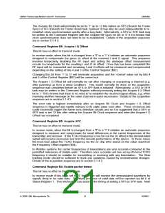
Command Register B6: Acquire I Q Offset
This bit has no effect in transmit mode.
In receive mode, when this bit is changed from a '0' to a '1' it initiates an automatic sequence
designed to compensate the gross dc offset of the received I and Q signal. This sequence
involves temporarily disabling the RF input and setting the analogue offset measurement
circuits to compensate for the resulting I and Q dc offset. Once this has been completed the
RF input will be reasserted and remaining I and Q offsets will be measured and compensated
depending on the setting of bits 4 and 5 of the Control Register ($02).
Changing this bit from ‘1’ to ‘0’ will terminate acquisition and the ‘normal’ value set by bits 4
and 5 of the Control Register ($02) will be carried out.
The Acquire I Q Offset bit will normally be set after changing or reacquiring a channel (e.g.
after powering up from a sleep condition). This would normally be done so the acquisition
sequence was completed before an SFS or SFH task is initiated. Alternatively, a SFS or SFH
task may be written to the Command Register without previously setting the Acquire I Q Offset
bit to ‘1’ if it is known that there is no need to re-establish the received signal offsets, e.g. when
receiving another message on the same channel in quick succession. Details of the acquisition
sequence are in section 5.1.4.3.
The error rate is highest immediately after an Acquire Bit Clock and Acquire I Q Offset
sequence is triggered and rapidly reduces to its static value soon after. These erroneous bits
could incorrectly trigger the frame sync detection circuits and so it is suggested that a SFH or
SFS task is set 12 bits after setting the Acquire Bit Clock sequence and when the Acquire I Q
Offset has completed.
Command Register B5: Acquire AFC
This bit has no effect in transmit mode.
In receive mode, when this bit is changed from a '0' to a '1' it initiates an automatic sequence
designed to measure and compensate for small differences in the carrier frequencies of the
transmitter and receiver. If the TCXO frequency is too far out the dc offset in the demodulated
signal will become excessive and limit the decode performance of the device. In these cases
the host must adjust the TCXO frequency via the on chip DAC based on the value read from
the Frequency Offset register ($04).
In Mobitex systems the carrier frequencies of basestations are very accurate compared to the
permitted tolerances of mobile units. Therefore once a mobile unit has set up it's local TCXO
frequency it should be suitable for transmitting or receiving with any basestation. The Slow
tracking mode should be sufficient to track any variations caused by environmental changes.
Details of the acquisition sequence are in section 5.1.4.3.
Command Register B4: Enable packet detect
This bit has no effect in transmit mode.
In receive mode if this bit is set to '1' the device will monitor the demodulated waveform for
signals likely to be valid data. The likely presence of valid data will be reported via bit 0 of
Status Register 1. This information can assist in the timing of setting a SFS or SFH task. Note
ã 2004 CML Microsystems Plc
21
D/990/1

 CMLMICRO [ CML MICROCIRCUITS ]