GMSK Packet Data Modem and RF Transceiver
CMX990
that some noise signals may appear in the baseband as valid data, the RSSI signal should be
used to confirm that the received signal is suitable before relying on this signal.
It is recommended that this bit is only set to ‘1’ when searching for the start of a packet. Once
a frame sync has been detected this bit should be set to ‘0’ until the start of a new packet
needs to be found.
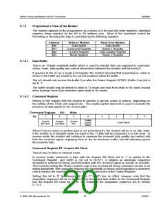
Command Register B3, B2, B1, B0: Task
Operations such as transmitting a data block are treated by the modem as ‘tasks’ and are
initiated when the µC writes a byte to the Command Register with the TASK bits set to one of
the data handling commands (marked BOLD in the table below).
Mobitex modem tasks:
B3 B2 B1 B0
Receive Mode
Transmit Mode
0
0
0
0
0
0
0
0
1
1
1
0
0
0
0
1
1
1
1
0
0
1
0
0
1
1
0
0
1
1
0
1
0
0
1
0
1
0
1
0
1
1
1
0
NULL
SFH
R3H
RDB
SFS
NULL
T7H
Search for Frame Head
Read 3 byte Frame Head
Read Data Block
Search for Frame Sync
Read Single Byte
Transmit 7 byte Frame Head
Reserved
Transmit Data Block
Transmit 4 Bytes
Transmit Single Byte
Transmit Scrambler Output
TDB
TQB
TSB
TSO
RSB
LFSB
Load Frame Sync Bytes
RESET Cancel any current action
SFHZ
RSD
RESET Cancel any current action
Reserved
TSD
SFH with zero errors
Read Short Data Block
SFS with zero errors
Transmit Short Data Block
Reserved
SFSZ
Note: All other bit patterns are reserved.
Bold text indicates a ‘data handling command’
The µC should not write a data handling command to the Command Register or write to or read
from the Data Buffer when the BFREE (Buffer Free) bit of the Status 1 Register is ‘0’.
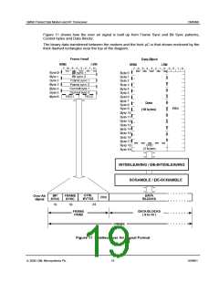
Different tasks apply in receive and transmit modes. Detailed timings for the various tasks are
given in Figures 14 and 15.
Transmit Operation
When the modem is in transmit mode, all data handling commands other than TSO instruct the
modem to transmit data from the Data Buffer, formatting it as required. For these tasks the µC
should wait until the BFREE (Buffer Free) bit of the Status 1 Register is ‘1’, before writing the
data to the Data Buffer. If more than 1 byte needs to be written to the Data Buffer, byte
number 0 of the block should be written first. The host should then write the desired task to the
Command Register.
Once the byte containing the desired task has been written to the Command Register, the
modem will:
Set the BFREE (Buffer Free) bit of the Status 1 Register to ‘0’.
Take the data from the Data Buffer as quickly as it can - transferring it to the Interleave
Buffer for eventual transmission. This operation will start immediately if the modem is
‘idle’ (i.e. not transmitting data from a previous task), otherwise it will be delayed until
there is sufficient room in the Interleave Buffer.
Once all of the data has been transferred from the Data Buffer the modem will set the
BFREE and IRQ bits of the Status 1 Register to ‘1’, (causing the chip IRQN output to go
low if the IRQ Enable bit of the Mode Register has been set to ‘1’) to tell the µC that it
may write new data and the next task to the modem.
ã 2004 CML Microsystems Plc
22
D/990/1

 CMLMICRO [ CML MICROCIRCUITS ]