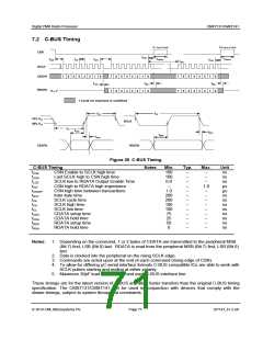
Digital PMR Radio Processor
CMX7131/CMX7141
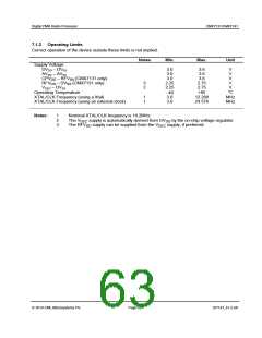
AC Parameters
Notes
Min.
Typ.
Max.
Unit
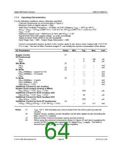
Modulator Outputs 1/2 and Audio Output
(MOD1, MOD2, AUDIO)
Power-up to Output Stable
Modulator Attenuators
Attenuation (at 0dB)
41
43
–
50
0
100
µs
+1.0
dB
1.0
Cumulative Attenuation Error
(wrt attenuation at 0dB)
Output Impedance
0
600
500
–
–
–
+0.6
–
–
dB
k
µA
V
0.6
–
–
–
0.5
20
42
42
Enabled
Disabled
Output Current Range (AV = 3.3V)
±125
DD
Output Voltage Range
Load Resistance
Audio Attenuator
Attenuation (at 0dB)
44
43
AV –0.5
DD
–
k
0
+1.0
dB
1.0
Cumulative Attenuation Error
(wrt attenuation at 0dB)
Output Impedance
0
600
500
–
–
–
+1.0
–
–
dB
k
µA
V
1.0
–
–
–
0.5
20
42
42
Enabled
Disabled
Output Current Range (AV = 3.3V)
±125
DD
Output Voltage Range
Load Resistance
44
AV –0.5
DD
–
k
41
Power-up refers to issuing a C-BUS command to turn on an output. These limits
apply only if V is on and stable. At power supply switch-on, the default state is
Notes:
BIAS
for all blocks, except the XTAL and C-BUS interface, to be in placed in Powersave
mode.
42
43
44
Small signal impedance, at AV = 3.3V and TAMB = 25°C.
With respect to the signal at the feedback pin of the selected input port.
DD
Centered about AV /2; with respect to the output driving a 20k load to AV /2.
DD
DD
2014 CML Microsystems Plc
Page 67
D/7141_FI-3.x/6

 CMLMICRO [ CML MICROCIRCUITS ]