Digital PMR Radio Processor
CMX7131/CMX7141
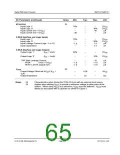
DC Parameters (continued)
Notes
Min.
Typ.
Max.
Unit
25
XTAL/CLK
Input Logic ‘1’
Input Logic ‘0’
Input Current (Vin = DV
Input Current (Vin = DV
70%
–
–
–
–
–
–
–
30%
40
DV
DV
µA
µA
DD
DD
)
)
DD
–
40
SS
C-BUS Interface and Logic Inputs
Input Logic ‘1’
70%
–
1.0
–
–
–
–
–
–
DV
DD
Input Logic ‘0’
Input Leakage Current (Logic ‘1’ or ‘0’)
Input Capacitance
30%
1.0
7.5
DV
DD
µA
pF
C-BUS Interface and Logic Outputs
Output Logic ‘1’
(I = 2mA)
90%
–
–
–
DV
OH
DD
Output Logic ‘0’
(I = -5mA)
OL
–
10%
DV
DD
“Off” State Leakage Current
IRQN (Vout = DV
REPLY_DATA (output HiZ)
–
1.0
1.0
–
–
–
10
+1.0
+1.0
µA
µA
µA
)
DD
26
V
BIAS
Output Voltage Offset wrt AV /2 (I
1A)
Output Impedance
<
–
–
±2%
22
–
–
AV
DD
DD
OL
k
25
26
Characteristics when driving the XTAL/CLK pin with an external clock source.
Notes:
Applies when utilising V
to provide a reference voltage to other parts of the
BIAS
system. When using V
as a reference, V
must be buffered. V
must
BIAS
BIAS
BIAS
always be decoupled with a capacitor as shown in Figure 2.
2014 CML Microsystems Plc
Page 65
D/7141_FI-3.x/6

 CMLMICRO [ CML MICROCIRCUITS ]