Digital PMR Radio Processor
CMX7131/CMX7141
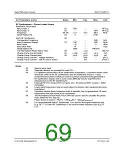
7.1.4 Parametric Performance
For the following conditions unless otherwise specified:
External components as recommended in Figure 2.
Maximum load on digital outputs = 30pF.
Oscillator Frequency = 19.2MHz 0.01% (100ppm); TAMB = 40°C to +85°C.
AV = DV = 3.0V to 3.6V.
DD
DD
Reference Signal Level = 308mVrms at 1kHz with AV = 3.3V.
DD
Signal levels track with supply voltage, so scale accordingly.
Signal-to-Noise Ratio (SNR) in Bit Rate Bandwidth.
Input Stage Gain = 0dB, Output Stage Attenuation = 0dB.
All figures quoted in this section apply to the device when loaded with FI3.x only. The use of
other Function Images™, can modify the parametric performance of the device.
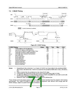
AC Parameters (cont.)
Modem Symbol Rate
Notes
Min.
2400
Typ.
–
Max.
4800
Unit
sym s-1
Modulation
Filter (RC) Alpha
Tx Output Level (MOD1, MOD2, 2-point)
Tx Output Level (MOD1, MOD2, I/Q)
Tx Adjacent Channel Power (MOD1, MOD2,
prbs)
4-FSK
0.2
2.88
2.20
–
–
–
–
–
–
–
–
70
70
71, 73
Vpk-pk
Vpk-pk
dB
-60
Rx Sensitivity (BER 4800 sym s-1)
Rx Co-channel Rejection
Rx System Adjacent Channel Rejection
(I/Q Mode)
72
71, 73
74
–
15
_
TBD
12
63
–
–
dBm
dB
dB
Rx Input Level
Rx Input DC Offset
–
0.5
–
–
838
mVrms
V
AV
-
DD
0.5
Notes:
70
71
72
73
74
Transmitting continuous default preamble.
See section 6.14.
Measured at base-band – radio design will affect ultimate product performance.
For a 6.25kHz/4800bps channel.
Combined performance of CMX7131/CMX7141 and CMX994 connected
as shown in Figure 6 using EV9942 and PE0201; measurement method
from EN 301 166.
2014 CML Microsystems Plc
Page 70
D/7141_FI-3.x/6

 CMLMICRO [ CML MICROCIRCUITS ]