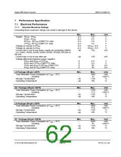
Digital PMR Radio Processor
CMX7131/CMX7141
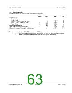
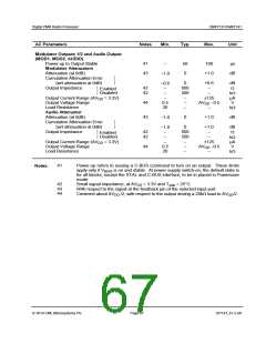
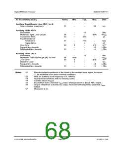
7.1.3 Operating Characteristics
For the following conditions unless otherwise specified:
External components as recommended in Figure 2.
Maximum load on digital outputs = 30pF.
Xtal/Clock Oscillator Frequency = 19.2MHz 0.01% (100ppm); TAMB = 40°C to +85°C.
AV = DV = CPV (CMX7131) = 3.0V to 3.6V; RFV (CMX7131) = 2.25V to 2.75V
DD
DD
DD
DD
V
DEC
= 2.5V
Reference Signal Level = 308mVrms at 1kHz with AV = 3.3V.
DD
Signal levels track with supply voltage, so scale accordingly.
Signal-to-Noise Ratio (SNR) in bit rate bandwidth.
Input Stage Gain = 0dB. Output Stage Attenuation = 0dB.
Current consumption figures quoted in this section apply to the device when loaded with 7131/7141
FI-3.x only. The use of other Function Images™, can modify the current consumption of the device.
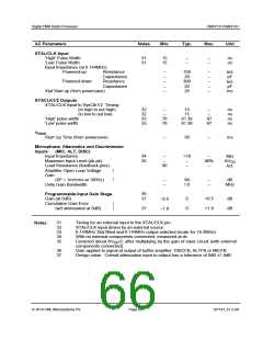
DC Parameters
Notes
Min.
Typ.
Max.
Unit
21
Supply Current
All Powersaved
DI
–
–
8
4
100
20
µA
µA
DD
AI
DD
22
Idle Mode
DI
–
–
1.4
1.6
–
–
mA
mA
DD
AI
DD
23
22
Rx Mode
DI (4800bps – search for FS)
–
–
–
4.7
2.8
1.6
–
–
–
mA
mA
mA
DD
DI (4800bps – FS found)
DD
AI
DD
22
Tx Mode
DI (4800bps – 2-point)
–
–
–
4.3
5.4
1.5
–
–
–
mA
mA
mA
DD
DI (4800bps – I/Q)
DD
AI (AV = 3.3V)
DD
DD
Additional Current for ach Auxiliary
System Clock (output running at 4MHz)
DI (DV = 3.3V, V = 2.5V)
–
–
–
–
250
50
–
–
µA
µA
µA
mA
DD
DD
DEC
Additional Current for Each Auxiliary ADC
DI (DV = 3.3V, V = 2.5V)
DD
DD
DEC
Additional Current for Each Auxiliary DAC
AI (AV = 3.3V)
200
2.5
–
DD
DD
24
Additional Current for Each RF Synthesiser
CPI + RFI (CPV = 3.3V, RFV = 2.5V)
4.5
DD
DD
DD
DD
21
22
TAMB =25°C. Not including any current drawn from the device pins by external
circuitry.
System clocks, auxiliary circuits disabled, but all other digital circuits (including the
Main Clock PLL) enabled.
Notes:
23
24
May be further reduced by power-saving unused sections
When using the external components shown in Figure 24 and when supplying the
current for RFV from the regulated 2.5V digital (V
) supply. The latter is
DEC
DD
derived from DV by an on-chip voltage regulator.
DD
2014 CML Microsystems Plc
Page 64
D/7141_FI-3.x/6

 CMLMICRO [ CML MICROCIRCUITS ]