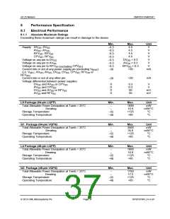
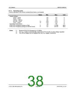
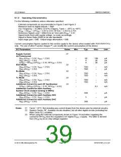
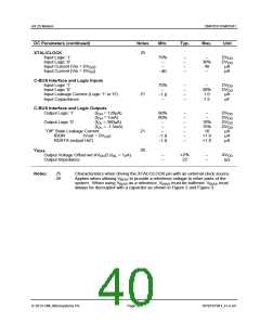
AX.25 Modem
CMX7031/CMX7041
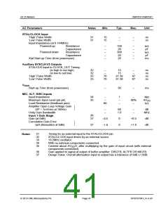
AC Parameters
Notes
Min.
Typ.
Max.
Unit
XTAL/CLOCK Input
‘High’ Pulse Width
‘Low’ Pulse Width
31
31
15
15
–
–
–
–
ns
ns
Input Impedance (at 6.144MHz)
Powered-up
Resistance
Capacitance
Resistance
Capacitance
–
–
–
–
–
150
20
300
20
20
–
–
–
–
–
k
pF
k
pF
ms
Powered-down
Xtal Start-up Time (from powersave)
Auxiliary SYSCLK1/2 Outputs
XTAL/CLK Input to CLOCK_OUT Timing:
(in high to out high)
32
32
33
33
–
–
76
76
15
15
81.38
81.38
–
–
87
87
ns
ns
ns
ns
(in low to out low)
‘High’ Pulse Width
‘Low’ Pulse Width
V
BIAS
Start-up Time (from powersave)
–
30
–
ms
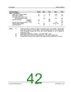
MIC, ALT, DISC Inputs
Input Impedance
34
35
–
–
80
1
–
–
–
80%
–
M
DD
k
Maximum Input Level (pk-pk)
Load Resistance (feedback pins)
Amplifier Open Loop Voltage Gain
(I/P = 1mVrms at 100Hz)
Unity Gain Bandwidth
AV
–
–
60
1.0
–
–
dB
MHz
36
37
Input 1 Gain Stage
Gain (at 0dB)
Cumulative Gain Error
(wrt attenuation at 0dB)
0
0
+0.5
+1.0
dB
dB
0.5
1.0
37
31
32
33
34
35
Timing for an external input to the XTAL/CLOCK pin.
XTAL/CLOCK input driven by an external source.
19.2MHz oscillator.
Notes:
With no external components connected.
Centred about AV /2; after multiplying by the gain of input circuit (with external
DD
components connected).
36
37
Gain applied to signal at output of buffer amplifier: DISCFB, ALTFB OR MICFB.
Design Value. Overall attenuation input to output has a tolerance of 0dB ±1.0dB.
2013 CML Microsystems Plc
Page 41
D/7031/7041_FI-4.x/5

 CMLMICRO [ CML MICROCIRCUITS ]