AX.25 Modem
CMX7031/CMX7041
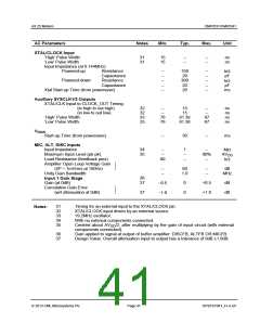
8.1.4 Parametric Performance
For the following conditions unless otherwise specified:
External components as recommended in Figure 2 and Figure 3.
Maximum load on digital outputs = 30pF.
Osc Frequency = 19.2MHz 0.01% (10ppm) ); Tamb = 40°C to +85°C.
AV = DV = CPV = 3.0V to 3.6V; RFVDD = 2.25V to 2.75V.
DD
DD
DD
Reference Signal Level = 308mVrms at 1kHz with AV = 3.3V.
DD
Signal levels track with supply voltage, so scale accordingly.
Signal to Noise Ratio (SNR) in bit rate bandwidth.
Input stage gain = 0dB, Output stage attenuation = 0dB.
All figures quoted in this section apply to the device when loaded with FI4.x only. The use of other
Function Images™, can modify the parametric performance of the device.
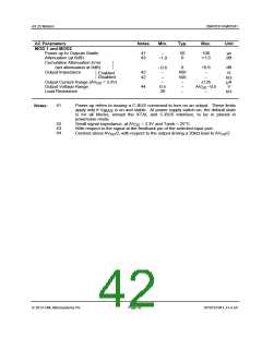
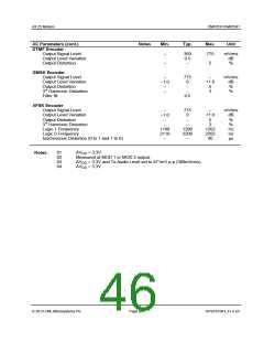
AC Parameters (cont.)
Notes
Min.
Typ.
Max.
Unit
Receiver Signal Type Identification
Probability of correctly identifying signal type
(SNR = 12dB)
–
>>99.9
–
%
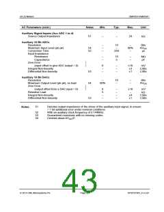
GMSK Decoder
Signal Input Dynamic Range
Bit Error Rate
Receiver Synchronisation
74
74
100
–
–
TBD
TBD
800
–
mVrms
10-8
(SNR = 20dB)
(SNR = 12dB)
AFSK Decoder
Signal Input Dynamic Range
Bit Error Rate
Receiver Synchronisation
74
74
100
–
–
TBD
TBD
800
–
mVrms
10-8
(SNR = 20dB)
(SNR = 12dB)
Notes:
74
AV
= 3.3V, for a “101010101 … 01” pattern measured at the input amplifier
DD
feedback pin. Signal level scales with AV
.
DD
2013 CML Microsystems Plc
Page 45
D/7031/7041_FI-4.x/5

 CMLMICRO [ CML MICROCIRCUITS ]