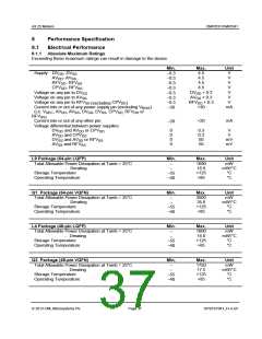
AX.25 Modem
CMX7031/CMX7041
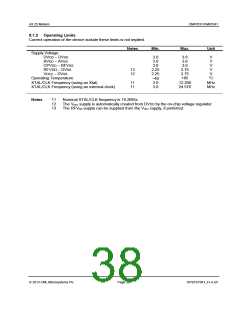
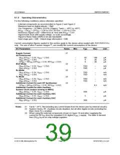
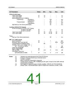
8.1.3 Operating Characteristics
For the following conditions unless otherwise specified:
External components as recommended in Figure 2 and Figure 3.
Maximum load on digital outputs = 30pF.
Osc Frequency = 19.2MHz 0.01% (10ppm); Tamb = 40°C to +85°C.
AV = DV = CPV = 3.0V to 3.6V; RFVDD = 2.25V to 2.75V.
DD
DD
DD
Reference Signal Level = 308mVrms at 1kHz with AV = 3.3V.
DD
Signal levels track with supply voltage, so scale accordingly.
Signal to Noise Ratio (SNR) in bit rate bandwidth.
Input stage gain = 0dB. Output stage attenuation = 0dB.
Current consumption figures quoted in this section apply to the device when loaded with 7031/7041FI-4.x
only. The use of other Function Images™, can modify the current consumption of the device.
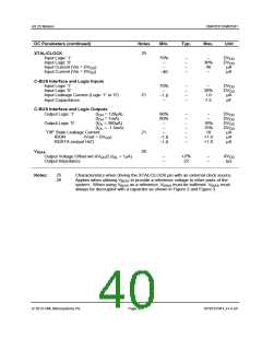
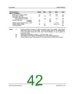
DC Parameters
Notes
Min.
Typ.
Max.
Unit
21
Supply Current
All Powersaved
DI (DV = 3.3V, V = 2.5V)
–
–
–
50
4
4
100
20
20
µA
µA
µA
DD
DD
DEC
AI (AV = 3.3V)
DD
DD
CPI + RFI (CPV = 3.3V, RFV = 2.5V)
DD
DD
DD
DD
22
22
22
23
IDLE Mode
DI (DV = 3.3V, V
= 2.5V)
= 2.5V)
= 2.5V)
–
–
TBD
TBD
–
–
mA
µA
DD
DD
DEC
DEC
DEC
AI (AV = 3.3V)
DD
DD
Rx Mode
DI (DV = 3.3V, V
–
–
TBD
TBD
–
–
mA
mA
DD
DD
AI (AV = 3.3V)
DD
DD
Tx Mode
DI (DV = 3.3V, V
–
–
TBD
TBD
–
–
mA
mA
DD
DD
AI (AV = 3.3V)
DD
DD
Additional Current for each RF Synthesiser
CPI + RFI (CPV = 3.3V, RFV = 2.5V)
–
4.5
mA
DD
DD
DD
DD
Additional Current for each Auxiliary
System Clock (output running at 4MHz)
DI (DV = 3.3V, V = 2.5V)
–
–
–
500
5
–
–
–
µA
µA
µA
DD
DD
DEC
Additional Current for each Auxiliary ADC
DI (DV = 3.3V, V = 2.5V)
DD
DD
DEC
Additional Current for each Auxiliary DAC
AI (AV = 3.3V)
200
DD
DD
21 Tamb = 25°C, Not including any current drawn from the device pins by external circuitry.
22 System Clocks, RF, Auxiliary circuits disabled, but all other digital circuits (including the
Main Clock PLL) enabled.
Notes:
23 When using the external components shown in Figure 16 and when supplying the
current for RFV from the regulated 2.5V digital (V
) supply. The latter is derived
DD
DEC
from DV by an on-chip voltage regulator.
DD
2013 CML Microsystems Plc
Page 39
D/7031/7041_FI-4.x/5

 CMLMICRO [ CML MICROCIRCUITS ]