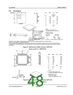
AX.25 Modem
CMX7031/CMX7041
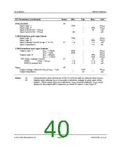
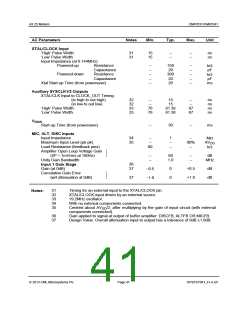
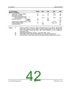
AC Parameters (cont.)
Notes
Min.
Typ.
Max.
Unit
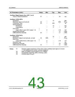
RF Synthesisers – Phase Locked Loops
Reference Clock Input
Input Logic ‘1’
Input Logic ‘0’
Frequency
62
62
64,66
63
70%
–
5.0
2
–
–
19.2
–
–
RFV
DD
30%
40.0
8191
RFV
DD
MHz
Divide Ratios (R)
Each RF Synthesiser
Comparison Frequency
Input Frequency Range
69
67
–
100
14
14
–
–
–
500
600
0
–
kHz
MHz
dBm
V/µs
Input Level
Input Slew Rate
–
Divide Ratios (N)
1088
–
1.88
470
–
–
1048575
1Hz Normalised Phase Noise Floor
Charge Pump Current (high)
Charge Pump Current (low)
Charge Pump Current – voltage variation
Charge Pump Current – sink to source match
68
65
65
–
3.3
820
–
dBc/Hz
mA
µA
per V
of ISET
197
2.5
625
10%
5%
–
–
Notes:
62
63
64
Square wave input.
Separate dividers are provided for each PLL.
For optimum performance of the synthesiser subsystems, a common master clock
should be used for the RF Synthesisers and the baseband sections. Using
unsynchronised clocks is likely to result in spurious products being generated in
the synthesiser outputs and in some cases difficulty may be experienced in
obtaining lock in the RF Synthesisers.
65
66
External ISET resistor (R31) = 0Ω (Internal ISET resistor = 9k6Ω nominally).
Lower input frequencies may be used subject to division ratio requirements being
maintained.
67
68
Operation outside these frequency limits is possible, but not guaranteed. Below
150MHz, a square wave input may be required to provide a fast enough slew rate.
1Hz Normalised Phase Noise Floor (PN1Hz) can be used to calculate the phase
noise within the PLL loop by:
Phase Noise (in-band) = PN1Hz + 20log10(N) + 10log10(fcomparison).
69
It is recommended that RF Synthesiser 1 be used for the higher frequency use
(eg: RF 1st LO) and RF Synthesiser 2 be used for lower frequency use (eg: IF LO).
2013 CML Microsystems Plc
Page 44
D/7031/7041_FI-4.x/5

 CMLMICRO [ CML MICROCIRCUITS ]