Calling Line Identifier with VMWI
CMX612
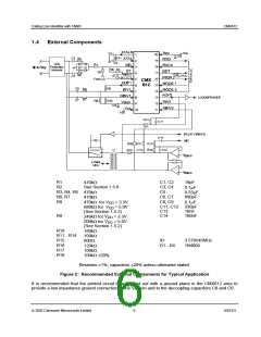
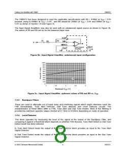
The CMX612 has been designed to meet the applicable specifications with R8 = 430kW at VDD = 3.0V
nominal, rising to 680kW at VDD = 5.0V, and R9 should be 240kW at VDD = 3.0V and 200kW at VDD
=
5.0V as shown in Section 1.4 and Figure 3c.
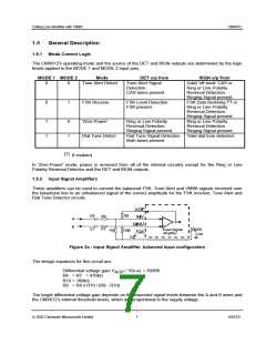
The Input Signal Amplifiers may also be used with an unbalanced signal source as shown in Figure 3b.
The values of R6 and R8 are as for the balanced input case.
Figure 3b : Input Signal Amplifier, unbalanced input configuration
1000
900
800
700
R8
600
500
400
300
R9
200
100
0
3
3.5
4
4.5
5
Nominal VDD (V)
Figure 3c : Input Signal Amplifier, optimum values of R8 and R9 vs. VDD
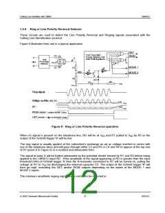
1.5.3 Bandpass Filters
These are used to attenuate out of band noise and interfering signals which might otherwise reach the
FSK Demodulator, Tone Alert Detector, Dial Tone detector and Level Detector circuits. The
characteristics of these filters differ in FSK, Tone Alert and Dial Tone modes. Most of the filtering is
provided by switched capacitor stages clocked at 57.7kHz or 9.62kHz depending on mode of operation.
1.5.4 Level Detector
This block operates by measuring the level of the signal at the output of the Bandpass Filter, and
comparing it against a threshold which depends on whether FSK Receive, Tone Alert Detect or Dial Tone
Detect mode has been selected.
In Tone Alert Detect mode the output of the Level Detector block provides an input to the Tone Alert
Signal Detector.
In Dial Tone Detect mode the output of the Level Detector block provides an input to the Dial Tone
Signal Detector.
ã 2002 Consumer Microcircuits Limited
8
D/612/3

 CMLMICRO [ CML MICROCIRCUITS ]