Calling Line Identifier with VMWI
CMX612
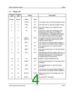
Package Package
Signal
Description
E3
P6
Pin No.
Pin No.
Name
Type
16
17
IRQN
O/P
An open-drain active low output that may be
used as an Interrupt Request/Wake-up input to
the associated mC. An external pull-up resistor
should be connected between this output and
VDD.
17
18
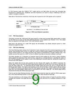
DET
O/P
A logic level output driven by the Ring or Line
Polarity Reversal Detector, the Tone Alert
Detector, the Dial Tone Detector or the FSK
Level detect circuits, depending on the
operating mode. See Section 1.5.1.
18
19
19
21
RXCK
RXD
I/P(S)
O/P
An input which may be used to clock received
data bits out of the FSK Data Retiming block.
A logic level output carrying either the raw
output of the FSK Demodulator or re-timed 8-bit
characters depending on the state of the RXCK
input. See Section 1.5.6.
20
22
VDD
Power
The positive supply rail. Levels and thresholds
within the device are proportional to this
voltage. Should be decoupled to VSS by a
capacitor mounted close to the device pins.
9, 20
Not used. Do not connect to these pins.
Notes: I/P
=
Input
I/P(S)= Schmitt trigger input
O/P = Output
BI
=
Bidirectional
ã 2002 Consumer Microcircuits Limited
5
D/612/3

 CMLMICRO [ CML MICROCIRCUITS ]