Calling Line Identifier with VMWI
CMX612
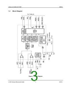
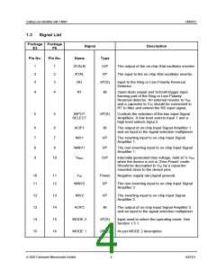
1.3
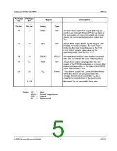
Signal List
Package Package
Signal
Description
E3
P6
Pin No.
Pin No.
Name
Type
O/P
1
2
3
1
2
3
XTALN
XTAL
RD
The output of the on-chip Xtal oscillator inverter.
The input to the on-chip Xtal oscillator inverter.
I/P
I/P(S)
Input to the Ring or Line Polarity Reversal
Detector.
4
4
RT
BI
Open-drain output and Schmitt trigger input
forming part of the Ring or Line Polarity
Reversal detector. An external resistor to VDD
and a capacitor to VSS should be connected to
RT to filter and extend the RD input signal.
5
5
INPUT
SELECT
I/P(S)
Controls the selection of the two Input Signal
Amplifiers. A low level selects Input 1 and a
high level selects Input 2.
6
7
8
9
6
7
AOP1
INV1
BI
I/P
The output of on-chip Input Signal Amplifier 1
and an input to the signal selection multiplexer.
The inverting input to on-chip Input Signal
Amplifier 1.
8
NINV1
VBIAS
I/P
The non-inverting input to on-chip Input Signal
Amplifier 1.
10
O/P
Internally generated bias voltage, held at ½ VDD
when the device is not in ‘Zero-Power’ mode.
Should be decoupled to VSS by a capacitor
mounted close to the device pins.
10
11
11
12
VSS
Power
I/P
Negative supply rail (signal ground).
NINV2
The non-inverting input to on-chip Input Signal
Amplifier 2.
12
13
14
15
13
14
15
16
INV2
I/P
BI
The inverting input to on-chip Input Signal
Amplifier 2.
AOP2
The output of on-chip Input Signal Amplifier 2
and an input to the signal selection multiplexer.
MODE 2
MODE 1
I/P(S)
I/P(S)
Input used to select the operating mode. See
Section 1.5.1.
As per MODE 2 description.
ã 2002 Consumer Microcircuits Limited
4
D/612/3

 CMLMICRO [ CML MICROCIRCUITS ]