Calling Line Identifier with VMWI
CMX612
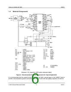
1.4
External Components
R1
R2
R3, R4, R5
R6, R7
R8
C1, C2
C3, C4
C5
C6, C7
C8, C9
C11, C12 330pF
C13
C14
18pF
470kW
See Section 1.5.8
470kW
470kW
470kW for VDD = 3.3V
680kW for VDD = 5.0V
(See Section 1.5.2)
240kW for VDD = 3.3V
200kW for VDD = 5.0V
(See Section 1.5.2)
160kW
0.1mF
0.33mF
680pF
0.1mF
10nF
100nF
R9
R10
R11 - R14
R15
R16
100kW
600W
120kW
X1
D1 - D4
3.579545MHz
1N4004
R17
100kW
R18
100kW ±20%
Resistors ±1%, capacitors ±20% unless otherwise stated.
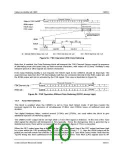
Figure 2 : Recommended External Components for Typical Application
It is recommended that the printed circuit board is laid out with a ground plane in the CMX612 area to
provide a low impedance ground connection to the VSS pin and to the decoupling capacitors C8 and C9.
ã 2002 Consumer Microcircuits Limited
6
D/612/3

 CMLMICRO [ CML MICROCIRCUITS ]