Calling Line Identifier with VMWI
CMX612
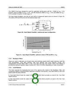
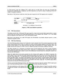
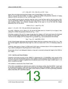
In FSK Receive mode the CMX612 DET output will be set high when the level has exceeded the
threshold for sufficient time. Amplitude and time hysteresis are used to reduce chattering of the DET
output in marginal conditions.
Note that in FSK Receive mode this circuit may also respond to non-FSK signals such as speech.
See Section 1.7.1 for definitions of Teon and Teoff
Figure 4 : FSK Level Detector operation
1.5.5 FSK Demodulator
This block converts the 1200 baud FSK input signal to a logic level received data signal which is output
via the RXD pin as long as the Data Retiming function is not enabled (see Section 1.5.6). This output
does not depend on the state of the FSK Level Detector output.
Note that in the absence of a valid FSK signal, the demodulator may falsely interpret speech or other
extraneous signals as data.
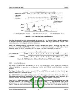
1.5.6 FSK Data Retiming
The Data Retiming block extracts the 8 data bits of each character from the received asynchronous data
stream, and presents them to the mC under the control of strobe pulses applied to the RXCK input. The
timing of these pulses is not critical and they may easily be generated by a simple software loop. This
facility removes the need for a UART in the mC without incurring an excessive software overhead.
The block operates on a character by character basis by first looking for the mark to space transition
which signals the beginning of the start bit, then, using this as a timing reference, sampling the output of
the FSK Demodulator in the middle of each of the following 8 received data bits, storing the results in an
internal 8-bit shift register.
When the eighth data bit has been clocked into the internal shift register, the CMX612 examines the
RXCK input. If this is low then the IRQN output will be pulled low and the first of the stored data bits put
onto the RXD output pin. On detecting that the IRQN output has gone low, the mC should pulse the
RXCK pin high 8 times. The high to low transition at the end of the first 7 of these pulses will be used by
the CMX612 to shift the next data bit from the shift register onto the RXD output. At the end of the eighth
pulse the FSK Demodulator output will be reconnected to the RXD output pin. The IRQN output will be
cleared the first time the RXCK input goes high.
Thus to use the Data Retiming function, the RXCK input should be kept low until the IRQN output goes
low; if the Data Retiming function is not required the RXCK input should be kept high.
The only restrictions on the timing of the RXCK waveform are those shown in Figure 5a and the need to
complete the transfer of all eight bits into the mC within 8.3ms (the time of a complete character at 1200
baud).
ã 2002 Consumer Microcircuits Limited
9
D/612/3

 CMLMICRO [ CML MICROCIRCUITS ]