CS49300 Family DSP
1.5. Switching Characteristics — RESET
(TA = 25 °C; VA, VD[3:1] = 2.5 V 5%; Inputs: Logic 0 = DGND, Logic 1 = VD, CL = 20 pF)
Parameter
Symbol
Min
Max
Unit
Trstl
100
-
µs
RESET minimum pulse width low (-CL)
RESET minimum pulse width low (-IL)
All bidirectional pins high-Z after RESET low
Configuration bits setup before RESET high
Configuration bits hold after RESET high
(Note 1)
(Note 1)
(Note 2)
Trstl
530
-
-
50
-
µs
ns
ns
ns
Trst2z
Trstsu
Trsthld
50
15
-
Notes: 1. The minimum RESET pulse listed above is valid only when using the recommended pull-up/pull-down
resistors on the RD, WR, PSEL and ABOOT mode pins. For Rev. D and older parts, pull-up/pull-down
resistors may be 4.7 k or 3.3 k. For Rev. E and newer parts, pull-up/pull-down resistors must be 3.3 k.
2. This specification is characterized but not production tested.
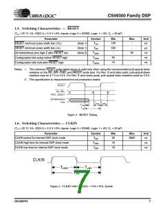
RESET
RD, W R,
PSEL, ABOOT
All Bidirectional
Pins
Trstsu Trsthld
Trst2z
Trstl
Figure 1. RESET Timing
1.6. Switching Characteristics — CLKIN
(TA = 25 °C; VA, VD[3:1] = 2.5 V 5%; Inputs: Logic 0 = DGND, Logic 1 = VD, CL = 20 pF)
Parameter
Symbol
Min
Max
Unit
CLKIN period for internal DSP clock mode
Tclki
35
3800
ns
CLKIN high time for internal DSP clock mode
CLKIN low time for internal DSP clock mode
Tclkih
Tclkil
18
18
ns
ns
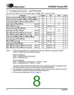
CLKIN
Tclkih
Tclkil
Tclki
Figure 2. CLKIN with CLKSEL = VSS = PLL Enable
DS339PP4
7

 CIRRUS [ CIRRUS LOGIC ]