CS49300 Family DSP
12.PIN DESCRIPTIONS ....................................................................................................... 80
13.ORDERING INFORMATION............................................................................................ 85
14.PACKAGE DIMENSIONS ............................................................................................... 85
LIST OF FIGURES
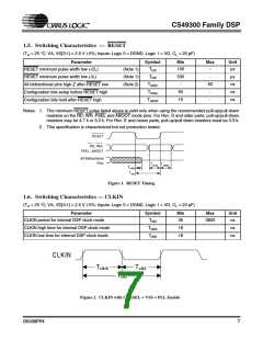
Figure 1. RESET Timing ..................................................................................................................... 7
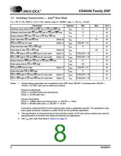
Figure 2. CLKIN with CLKSEL = VSS = PLL Enable .......................................................................... 7
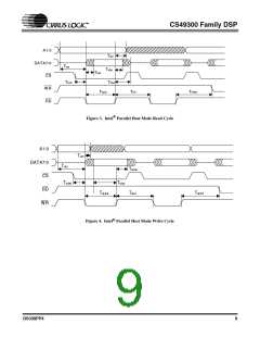
Figure 3. Intel® Parallel Host Mode Read Cycle ................................................................................. 9
Figure 4. Intel® Parallel Host Mode Write Cycle ................................................................................. 9
Figure 5. Motorola® Parallel Host Mode Read Cycle ........................................................................ 11
Figure 6. Motorola® Parallel Host Mode Write Cycle ........................................................................ 11
Figure 7. SPI Control Port Timing ..................................................................................................... 13
Figure 8. I2C® Control Port Timing ................................................................................................... 15
Figure 9. Digital Audio Input Data, Master and Slave Clock Timing ................................................. 17
Figure 10. Serial Compressed Data Timing ...................................................................................... 18
Figure 11. Parallel Data Timing (when not in a parallel control mode) ............................................. 18
Figure 12. Digital Audio Output Data, Input and Output Clock Timing ............................................. 20
Figure 13. I2C® Control ..................................................................................................................... 26
Figure 14. I2C® Control with External Memory ................................................................................. 27
Figure 15. SPI Control ...................................................................................................................... 28
Figure 16. SPI Control with External Memory ................................................................................... 29
Figure 17. Intel® Parallel Control Mode ............................................................................................ 30
Figure 18. Motorola® Parallel Control Mode ..................................................................................... 31
Figure 19. SPI Write Flow Diagram .................................................................................................. 33
Figure 20. SPI Read Flow Diagram .................................................................................................. 34
Figure 21. SPI Timing ....................................................................................................................... 36
Figure 22. I2C® Write Flow Diagram ................................................................................................ 37
Figure 23. I2C® Read Flow Diagram ................................................................................................ 38
Figure 24. I2C® Timing ..................................................................................................................... 40
Figure 24. Intel Mode, One-Byte Write Flow Diagram ...................................................................... 44
Figure 25. Intel Mode, One-Byte Read Flow Diagram ...................................................................... 44
Figure 26. Motorola Mode, One-Byte Write Flow Diagram ............................................................... 45
Figure 27. Motorola Mode, One-Byte Read Flow Diagram ............................................................... 46
Figure 28. Typical Parallel Host Mode Control Write Sequence Flow Diagram ............................... 47
Figure 29. Typical Parallel Host Mode Control Read Sequence Flow Diagram ............................... 48
Figure 30. External Memory Interface .............................................................................................. 51
Figure 31. External Memory Read (16-bit address) ......................................................................... 51
Figure 32. External Memory Write (16-bit address) .......................................................................... 51
Figure 33. Typical Serial Boot and Download Procedure ................................................................. 53
Figure 34. Typical Parallel Boot and Download Procedure .............................................................. 54
Figure 35. Autoboot Timing Diagram ................................................................................................ 56
Figure 37. Autoboot INTREQ Behavior ............................................................................................ 57
Figure 36. Autoboot Sequence ......................................................................................................... 58
4
DS339PP4

 CIRRUS [ CIRRUS LOGIC ]