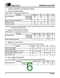
CS49300 Family DSP
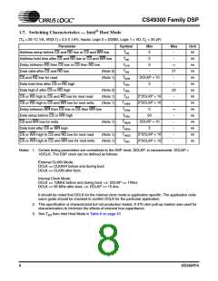
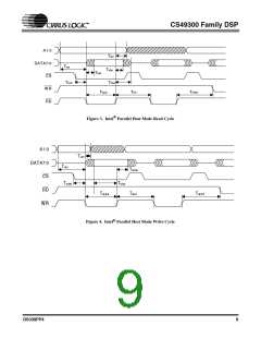
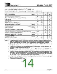
1.8. Switching Characteristics — Motorola® Host Mode
(TA = 25 °C; VA, VD[3:1] = 2.5 V 5%; Inputs: Logic 0 = DGND, Logic 1 = VD, CL = 20 pF)
Parameter
Symbol
Min
Max
Unit
Tmas
5
-
ns
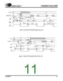
Address setup before CS and DS low
Tmah
Tmcdr
Tmdd
5
0
-
-
ns
ns
ns
Address hold time after CS and DS low
Delay between DS then CS low or CS then DS low
Data valid after CS and RD low with R/W high
∞
21
(Note 3)
(Note 1)
Tmrpw
Tmdhr
DCLKP + 10
-
-
ns
ns
ns
ns
ns
ns
ns
ns
ns
ns
ns
ns
CS and DS low for read
5
Data hold time after CS or DS high after read
Data high-Z after CS or DS high low after read
CS or DS high to CS and DS low for next read
CS or DS high to CS and DS low for next write
Delay between DS then CS low or CS then DS low
Data setup before CS or DS high
Tmdis
-
22
-
(Note 2)
(Note 1)
(Note 1)
Tmrd
2*DCLKP + 10
Tmrdtw
Tmcdw
Tmdsu
Tmwpw
Tmrwsu
Tmrwhld
Tmdhw
Tmwtrd
2*DCLKP + 10
-
0
∞
-
20
DCLKP + 10
-
CS and DS low for write
(Note 1)
5
-
R/W setup before CS AND DS low
R/W hold time after CS or DS high
Data hold after CS or DS high
5
-
5
-
2*DCLKP + 10
-
CS or DS high to CS and DS low with R/W high for next read
(Note 1)
Tmwd
2*DCLKP + 10
-
ns
CS or DS high to CS and DS low for next write
(Note 1)
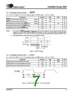
Notes: 1. Certain timing parameters are normalized to the DSP clock, DCLKP, in nanoseconds. DCLKP =
1/DCLK. The DSP clock can be defined as follows:
External CLKIN Mode:
DCLK == CLKIN/4 before and during boot
DCLK == CLKIN after boot
Internal Clock Mode:
DCLK == 10MHz before and during boot, i.e. DCLKP == 100ns
DCLK == 65 MHz after boot, i.e. DCLKP == 15.4ns
It should be noted that DCLK for the internal clock mode is application specific. The application code
users guide should be checked to confirm DCLK for the particular application.
2. This specification is characterized but not production tested. A 470 ohm pull-up resistor was used for
characterization to minimize the effects of external bus capacitance.
3. See Tmdd from Motorola Host Mode in Table 7 on page 45
10
DS339PP4

 CIRRUS [ CIRRUS LOGIC ]