CS4365
2
3.14.2.1 I C Write
To write to the device, follow the procedure below while adhering to the control port Switching Specifi-
cations in section 2.
2
1. Initiate a START condition to the I C bus followed by the address byte. The upper 6 bits must be
001100. The seventh bit must match the setting of the AD0 pin, and the eighth must be 0. The eighth
bit of the address byte is the R/W bit.
2. Wait for an acknowledge (ACK) from the part, then write to the memory address pointer, MAP. This
byte points to the register to be written.
3. Wait for an acknowledge (ACK) from the part, then write the desired data to the register pointed to
by the MAP.
4. If the INCR bit (see section 3.14.1) is set to 1, repeat the previous step until all the desired registers
are written, then initiate a STOP condition to the bus.
2
5. If the INCR bit is set to 0 and further I C writes to other registers are desired, it is necessary to ini-
tiate a repeated START condition and follow the procedure detailed from step 1. If no further writes to
other registers are desired, initiate a STOP condition to the bus.
2
3.14.2.2 I C Read
To read from the device, follow the procedure below while adhering to the control port Switching Spec-
ifications.
2
1. Initiate a START condition to the I C bus followed by the address byte. The upper 6 bits must be
001100. The seventh bit must match the setting of the AD0 pin, and the eighth must be 1. The eighth
bit of the address byte is the R/W bit.
2. After transmitting an acknowledge (ACK), the device will then transmit the contents of the register
pointed to by the MAP. The MAP register will contain the address of the last register written to the MAP,
2
or the default address (see section 3.14.1) if an I C read is the first operation performed on the device.
3. Once the device has transmitted the contents of the register pointed to by the MAP, issue an ACK.
4. If the INCR bit is set to 1, the device will continue to transmit the contents of successive registers.
Continue providing a clock and issue an ACK after each byte until all the desired registers are read, then
initiate a STOP condition to the bus.
2
5. If the INCR bit is set to 0 and further I C reads from other registers are desired, it is necessary to
2
initiate a repeated START condition and follow the procedure detailed from steps 1 and 2 from the I C
2
Write instructions followed by step 1 of the I C Read section. If no further reads from other registers are
desired, initiate a STOP condition to the bus.
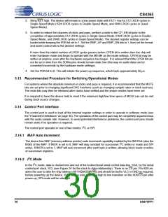
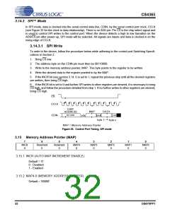
Note 1
ADDR
AD0
DATA
1-8
DATA
1-8
001100
R/W
ACK
ACK
ACK
SDA
SCL
Start
Stop
Note: If operation is a write, this byte contains the Memory Address Pointer, MAP.
Figure 24. Control Port Timing, I2C Mode
DS670PP1
31

 CIRRUS [ CIRRUS LOGIC ]