CS4365
3.11 The MUTEC Outputs
The MUTEC1-6 pins have an auto-polarity detect feature. The MUTEC output pins are high impedance at the time
of reset. The external mute circuitry needs to be self biased into an active state in order to be muted during reset.
Upon release of reset, the CS4365 will detect the status of the MUTEC pins (high or low) and will then select that
state as the polarity to drive when the mutes become active. The external-bias voltage level that the MUTEC pins
see at the time of release of reset must meet the “MUTEC auto detect input high/low voltage” specs as outlined in
the Digital Characteristics section.
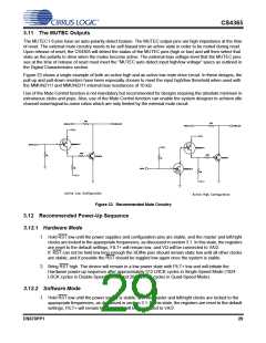
Figure 23 shows a single example of both an active high and an active low mute drive circuit. In these designs, the
pull-up and pull-down resistors have been especially chosen to meet the input high/low threshold when used with
the MMUN2111 and MMUN2211 internal bias resistances of 10 kΩ.
Use of the Mute Control function is not mandatory but recommended for designs requiring the absolute minimum in
extraneous clicks and pops. Also, use of the Mute Control function can enable the system designer to achieve idle
channel noise/signal-to-noise ratios which are only limited by the external mute circuit.
Figure 23. Recommended Mute Circuitry
3.12 Recommended Power-Up Sequence
3.12.1 Hardware Mode
1. Hold RST low until the power supplies and configuration pins are stable, and the master and left/right
clocks are locked to the appropriate frequencies, as discussed in section 3.1. In this state, the registers
are reset to the default settings, FILT+ will remain low, and VQ will be connected to VA/2.
If RST can not be held low long enough the SDINx pins should remain static low until all other clocks
are stable, and if possible the RST should be toggled low again once the system is stable.
2. Bring RST high. The device will remain in a low power state with FILT+ low and will initiate the
Hardware power-up sequence after approximately 512 LRCK cycles in Single-Speed Mode (1024
LRCK cycles in Double-Speed Mode, and 2048 LRCK cycles in Quad-Speed Mode).
3.12.2 Software Mode
1. Hold RST low until the power supply is stable, and the master and left/right clocks are locked to the
appropriate frequencies, as discussed in section 3.1. In this state, the registers are reset to the default
settings, FILT+ will remain low, and VQ will be connected to VA/2.
DS670PP1
29

 CIRRUS [ CIRRUS LOGIC ]