CAT24WC257
SDA: Serial Data/Address
FUNCTIONAL DESCRIPTION
The bidirectional serial data/address pin is used to
transfer all data into and out of the device. The SDA pin
is an open drain output and can be wire-ORed with other
open drain or open collector outputs.
The CAT24WC257 supports the I2C Bus data transmis-
sion protocol. This Inter-Integrated Circuit Bus protocol
defines any device that sends data to the bus to be a
transmitter and any device receiving data to be a re-
ceiver. The transfer is controlled by the Master device
which generates the serial clock and all START and
STOP conditions for bus access. The CAT24WC257
operates as a Slave device. Both the Master device and
Slave device can operate as either transmitter or re-
ceiver, but the Master device controls which mode is
activated.
WP: Write Protect
This input, when tied to GND, allows write operations to
the entire memory. When this pin is tied to Vcc, the top
1/4 array of memory (locations 6000H to 7FFFH) is write
protected. When left floating, memory is unprotected.
A0, A1: Device Address Inputs
These pins are hardwired or left connected. When
hardwired,uptofourCAT24WC257'smaybeaddressed
on a single bus system. When the pins are left uncon-
nected, the default values are zero.
PIN DESCRIPTIONS
SCL: Serial Clock
The serial clock input clocks all data transferred into or
out of the device.
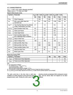
Figure 1. Bus Timing
t
t
t
F
HIGH
R
t
t
LOW
LOW
SCL
t
t
HD:DAT
SU:STA
t
t
t
t
HD:STA
SU:DAT
SU:STO
BUF
SDA IN
t
t
DH
AA
SDA OUT
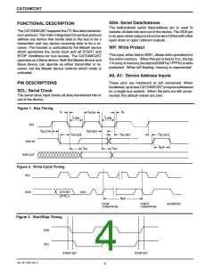
Figure 2. Write Cycle Timing
SCL
SDA
8TH BIT
BYTE n
ACK
t
WR
STOP
CONDITION
START
CONDITION
ADDRESS
Figure 3. Start/Stop Timing
SDA
SCL
START BIT
STOP BIT
Doc. No. 1030, Rev. E
4

 CATALYST [ CATALYST SEMICONDUCTOR ]