CAT24WC257
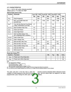
A.C. CHARACTERISTICS
= +1.8V to +6V, unless otherwise specified
V
CC
Output Load is 1 TTL Gate and 100pF
Read & Write Cycle Limits
Symbol Parameter
VCC=1.8V - 6.0V VCC=2.5V - 6.0V VCC=3.0V - 5.5V
Min
Max
100
3.5
Min
Max
400
0.9
Min
Max
1000
0.55
Units
kHz
µs
FSCL
tAA
Clock Frequency
SCL Low to SDA Data Out
and ACK Out
0.1
0.05
1.2
0.05
0.5
(1)
tBUF
Time the Bus Must be Free Before 4.7
a New Transmission Can Start
µs
tHD:STA
tLOW
Start Condition Hold Time
Clock Low Period
4.0
4.7
4.0
4.0
0.6
1.2
0.6
0.6
0.25
0.6
µs
µs
µs
µs
tHIGH
Clock High Period
0.4
tSU:STA
Start Condition Setup Time
(for a Repeated Start Condition)
0.25
tHD:DAT
tSU:DAT
Data In Hold Time
0
0
0
ns
ns
µs
ns
µs
ns
ms
Data In Setup Time
100
100
100
(1)
tR
SDA and SCL Rise Time
SDA and SCL Fall Time
Stop Condition Setup Time
Data Out Hold Time
Write Cycle Time
1.0
0.3
0.3
(1)
tF
300
300
100
tSU:STO
tDH
4.7
0.6
50
0.25
50
100
tWR
10
10
10
(2)(3)
Power-Up Timing
Symbol Parameter
Min
Typ
Max
1
Units
ms
tPUR
tPUW
Power-Up to Read Operation
Power-Up to Write Operation
1
ms
Note:
(1) AC measurement conditions:
RL (connects to V ): 0.3V to 0.7 V
CC
CC
CC
Input rise and fall times: < 50ns
Input and output timeing reference voltages: 0.5 V
CC
(2) This parameter is tested initially and after a design or process change that affects the parameter.
(3) t and t are the delays required from the time V is stable until the specified operation can be initiated.
PUR
PUW
CC
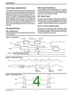
interface circuits are disabled, SDA is allowed to remain
high, and the device does not respond to its slave
address.
The write cycle time is the time from a valid stop
condition of a write sequence to the end of the internal
program/erase cycle. During the write cycle, the bus
Doc. No. 1030, Rev. E
3

 CATALYST [ CATALYST SEMICONDUCTOR ]