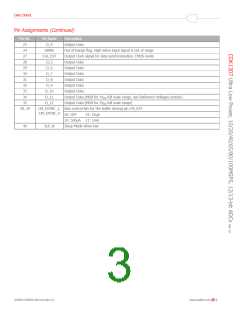
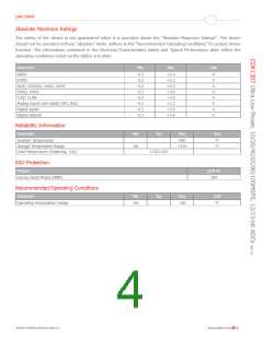
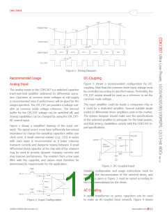
Data Sheet
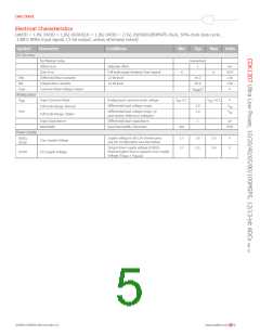
Electrical Characteristics - CDK1307B
(AVDD = 1.8V, DVDD = 1.8V, DVDDCLK = 1.8V, OVDD = 2.5V, 40MSPS clock, 50% clock duty cycle,
-1dBFS 8MHz input signal, 13-bit output, unless otherwise noted)
Symbol
Parameter
Conditions
Min
Typ
Max
Units
Performance
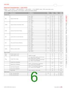
FIN = 2MHz
FIN = 8MHz
FIN ≃ FS/2
72.5
72.7
72
dBFS
dBFS
dBFS
dBFS
dBFS
dBFS
dBFS
dBFS
dBc
71.9
SNR
Signal to Noise Ratio
FIN = 30MHz
FIN = 2MHz
FIN = 8MHz
FIN ≃ FS/2
70.8
71.7
72.1
71.5
71.2
81
71
75
SINAD
SFDR
HD2
Signal to Noise and Distortion Ratio
Spurious Free Dynamic Range
Second order Harmonic Distortion
Third order Harmonic Distortion
Effective number of Bits
FIN = 30MHz
FIN = 2MHz
FIN = 8MHz
FIN ≃ FS/2
81
dBc
80
dBc
FIN = 30MHz
FIN = 2MHz
FIN = 8MHz
FIN ≃ FS/2
80
dBc
-90
-95
-95
-90
-81
-81
-80
-80
11.6
11.7
11.6
11.4
dBc
-85
dBc
dBc
FIN = 30MHz
FIN = 2MHz
FIN = 8MHz
FIN ≃ FS/2
dBc
dBc
dBc
HD3
-75
dBc
FIN = 30MHz
FIN = 2MHz
FIN = 8MHz
FIN ≃ FS/2
dBc
bits
11.5
bits
ENOB
bits
FIN = 30MHz
bits
Power Supply
AIDD
Analog Supply Current
Digital Supply Current
13.4
1.7
mA
mA
mA
DIDD
Digital core supply
2.5V output driver supply, sine wave input,
FIN = 1MHz, CLK_EXT enabled
3.3
OIDD
Output Driver Supply
2.5V output driver supply, sine wave input,
FIN = 1MHz, CLK_EXT disabled
2.4
mA
Analog Power Dissipation
Digital Power Dissipation
24.1
9.1
mW
mW
OVDD = 2.5V, 5pF load on output bits,
FIN = 1MHz, CLK_EXT disabled
OVDD = 2.5V, 5pF load on output bits,
FIN = 1MHz, CLK_EXT disabled
33.2
mW
Total Power Dissipation
Power Down Dissipation
Sleep Mode
9.7
μW
Power Dissipation, Sleep mode
14.2
mW
Clock Inputs
Max. Conversion Rate
Min. Conversion Rate
40
MSPS
MSPS
20
©2009 CADEKA Microcircuits LLC
www.cadeka.com
7

 CADEKA [ CADEKA MICROCIRCUITS LLC. ]