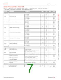
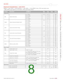
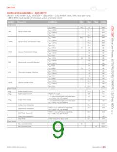
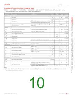
Data Sheet
N+4
N+3
N+5
N+2
N+1
N
N-13
CLK_EXT
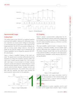
Figure 1. Timing Diagram
Recommended Usage
Analog Input
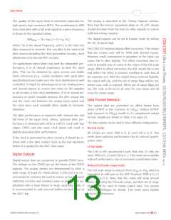
DC-Coupling
Figure 3 shows a recommended configuration for DC-
coupling. Note that the common mode input voltage must
be controlled according to specified values. Preferably, the
CM_EXT output should be used as a reference to set the
common mode voltage.
The analog inputs to the CDK1307 is a switched capacitor
track-and-hold amplifier optimized for differential opera-
tion. Operation at common mode voltages at mid supply
is recommended even if performance will be good for the
ranges specified. The CM_EXT pin provides a voltage suit-
able as common mode voltage reference. The internal
buffer for the CM_EXT voltage can be switched off, and
driving capabilities can be changed by using the CM_EXT-
BC control input.
The input amplifier could be inside a companion chip or
it could be a dedicated amplifier. Several suitable single
ended to differential driver amplifiers exist in the market.
The system designer should make sure the specifications
of the selected amplifier is adequate for the total system,
and that driving capabilities comply with the CDK1307 in-
put specifications.
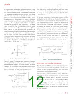
Figure 2 shows a simplified drawing of the input net-
work. The signal source must have sufficiently low output
impedance to charge the sampling capacitors within one
clock cycle. A small external resistor (e.g. 22Ω) in series
with each input is recommended as it helps reducing
transient currents and dampens ringing behavior. A small
differential shunt capacitor at the chip side of the resistors
may be used to provide dynamic charging currents and
may improve performance. The resistors form a low pass
filter with the capacitor, and values must therefore be
determined by requirements for the application.
43Ω
33pF
43Ω
Figure 3. DC-Coupled Input
Detailed configuration and usage instructions must be
found in the documentation of the selected driver, and
the values given in Figure 3 must be varied according to
the recommendations for the driver.
AC-Coupling
A signal transformer or series capacitors can be used
to make an AC-coupled input network. Figure 4 shows
Figure 2. Input Configuration
©2009 CADEKA Microcircuits LLC
www.cadeka.com
11

 CADEKA [ CADEKA MICROCIRCUITS LLC. ]