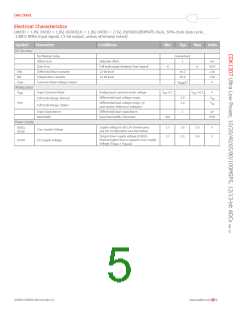
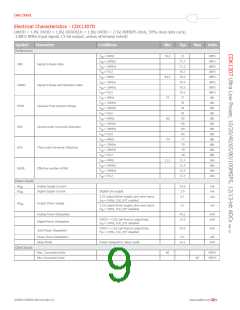
Data Sheet
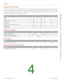
Electrical Characteristics
(AVDD = 1.8V, DVDD = 1.8V, DVDDCLK = 1.8V, OVDD = 2.5V, 20/40/65/80MSPS clock, 50% clock duty cycle,
-1dBFS 8MHz input signal, 13-bit output, unless otherwise noted)
Symbol
Parameter
Conditions
Min
Typ
Max
Units
DC Accuracy
No Missing Codes
Guaranteed
1
Offset Error
Midscale offset
mV
%FS
LSB
LSB
V
Gain Error
Full scale range deviation from typical
12-bit level
-6
6
DNL
Differential Non-Linearity
Integral Non-Linearity
Common Mode Voltage Output
±0.2
±0.6
INL
12-bit level
VCMO
VAVDD/2
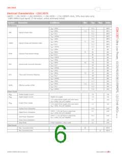
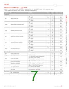
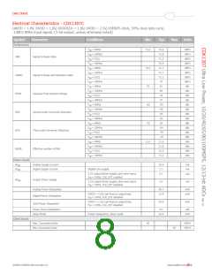
Analog Input
VCMI
Input Common Mode
Analog input common mode voltage
Differential input voltage range,
VCM -0.1
VCM +0.2
V
2.0
1.0
Vpp
Vpp
Full Scale Range, Normal
VFSR
Differential input voltage range, 1V
(see section Reference Voltages)
Full Scale Range, Option
Input Capacitance
Bandwidth
Differential input capacitance
Input bandwidth, full power
2
pF
500
MHz
Power Supply
Supply voltage to all 1.8V domain pins.
See Pin Configuration and Description
1.7
1.7
1.8
2.5
2.0
3.6
V
V
AVDD,
DVDD
Core Supply Voltage
I/O Supply Voltage
Output driver supply voltage (OVDD).
Must be higher than or equal to Core Supply
OVDD
Voltage (VOVDD ≥ VOCVDD
)
©2009 CADEKA Microcircuits LLC
www.cadeka.com
5

 CADEKA [ CADEKA MICROCIRCUITS LLC. ]