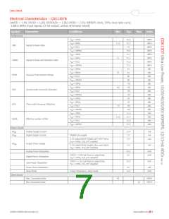
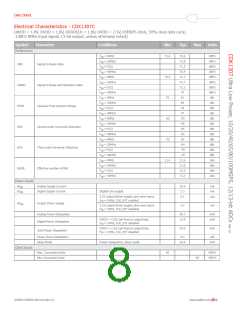
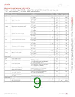
Data Sheet
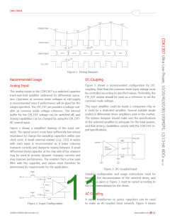
The quality of the input clock is extremely important for The timing is described in the Timing Diagram section.
Note that the load or equivalent delay on CK_EXT always
should be lower than the load on data outputs to ensure
sufficient timing margins.
high-speed, high-resolution ADCs. The contribution to SNR
from clock jitter with a full scale signal at a given frequency
is shown in the equation below:
The digital outputs can be set in tristate mode by setting
the OE_N signal high.
•
•
•
•
SNR
= 20 log (2 π F εt)
jitter
IN
where F is the signal frequency, and εt is the total rms
IN
The CDK1307 employs digital offset correction. This means
that the output code will be 4096 with shorted inputs.
However, small mismatches in parasitics at the input can
cause this to alter slightly. The offset correction also re-
sults in possible loss of codes at the edges of the full scale
range. With no offset correction, the ADC would clip in one
end before the other, in practice resulting in code loss at
the opposite end. With the output being centered digitally,
the output will clip, and the out of range flags will be set,
before max code is reached. When out of range flags are
set, the code is forced to all ones for over-range and all
zeros for under-range.
jitter measured in seconds. The rms jitter is the total of all
jitter sources including the clock generation circuitry, clock
distribution and internal ADC circuitry.
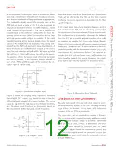
For applications where jitter may limit the obtainable per-
formance, it is of utmost importance to limit the clock
jitter. This can be obtained by using precise and stable
clock references (e.g. crystal oscillators with good jitter
specifications) and make sure the clock distribution is well
controlled. It might be advantageous to use analog power
and ground planes to ensure low noise on the supplies
to all circuitry in the clock distribution. It is of utmost im-
portance to avoid crosstalk between the ADC output bits
and the clock and between the analog input signal and
the clock since such crosstalk often results in harmonic
distortion.
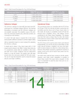
Data Format Selection
The output data are presented on offset binary form
when DFRMT is low (connect to OV ). Setting DFRMT
SS
high (connect to OV ) results in 2’s complement output
DD
The jitter performance is improved with reduced rise and
fall times of the input clock. Hence, optimum jitter per-
formance is obtained with LVDS or LVPECL clock with fast
edges. CMOS and sine wave clock inputs will result in
slightly degraded jitter performance.
format. Details are shown in Table 1 on page 14.
The data outputs can be used in three different configurations.
Normal mode:
All 13-bits are used. MSB is D_12 and LSB is D_0. This
mode gives optimum performance due to reduced quanti-
zation noise.
If the clock is generated by other circuitry, it should be re-
timed with a low jitter master clock as the last operation
before it is applied to the ADC clock input.
12-bit mode:
The LSB is left unconnected such that only 12 bits are
used. MSB is D_12 and LSB is D_1. This mode gives slightly
reduced performance, due to increased quantization noise.
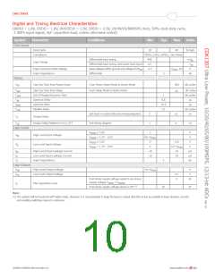
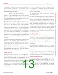
Digital Outputs
Digital output data are presented on parallel CMOS form.
The voltage on the OVDD pin set the levels of the CMOS
outputs. The output drivers are dimensioned to drive a
wide range of loads for OVDD above 2.25V, but it is rec-
ommended to minimize the load to ensure as low transient
switching currents and resulting noise as possible. In ap-
plications with a large fanout or large capacitive loads, it
is recommended to add external buffers located close to
the ADC chip.
Reduced full scale range mode:
The full scale range is reduced from 2V to 1V which is
pp
pp
equivalent to 6dB gain in the ADC frontend. MSB is D_11
and LSB is D_0. Note that the codes will wrap around
when exceeding the full scale range, and that out of range
bits should be used to clamp output data. See section
Reference Voltages for details. This mode gives slightly
reduced performance.
©2009 CADEKA Microcircuits LLC
www.cadeka.com
13

 CADEKA [ CADEKA MICROCIRCUITS LLC. ]