BSI
BS62UV1024
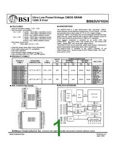
PIN DESCRIPTIONS
Name
Function
A0-A16 Address Input
These 17 address inputs select one of the 131,072 x 8-bit words in the RAM
CE1 Chip Enable 1 Input
CE2 Chip Enable 2 Input
CE1 is active LOW and CE2 is active HIGH. Both chip enables must be active when
data read from or write to the device. If either chip enable is not active, the device is
deselected and is in a standby power mode. The DQ pins will be in the high
impedance state when the device is deselected.
WE Write Enable Input
OE Output Enable Input
The write enable input is active LOW and controls read and write operations. With the
chip selected, when WE is HIGH and OE is LOW, output data will be present on the
DQ pins; when WE is LOW, the data present on the DQ pins will be written into the
selected memory location.
The output enable input is active LOW. If the output enable is active while the chip is
selected and the write enable is inactive, data will be present on the DQ pins and they
will be enabled. The DQ pins will be in the high impedance state when OE is inactive.
These 8 bi-directional ports are used to read data from or write data into the RAM.
DQ0-DQ7 Data Input/Output
Ports
Vcc
Power Supply
Ground
Gnd
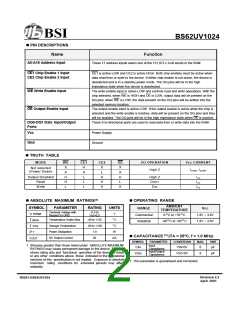
TRUTH TABLE
MODE
WE
X
X
CE1
H
X
CE2
X
L
OE
X
X
I/O OPERATION
Vcc CURRENT
Not selected
High Z
I
CCSB, ICCSB1
(Power Down)
Output Disabled
Read
H
H
L
L
L
L
H
H
H
H
L
X
High Z
DOUT
DIN
ICC
ICC
ICC
Write
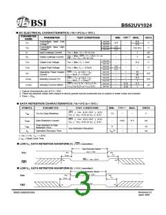
ABSOLUTE MAXIMUM RATINGS(1)
OPERATING RANGE
AMBIENT
TEMPERATURE
0 O C to +70 O
-40 O C to +85O
SYMBOL
PARAMETER
RATING
UNITS
RANGE
Vcc
Terminal Voltage with
Respect to GND
-0.5 to
V
TERM
BIAS
STG
T
V
T
T
P
Commercial
Industrial
C
1.8V ~ 3.6V
1.8V ~ 3.6V
Vcc+0.5
Temperature Under Bias
Storage Temperature
Power Dissipation
-40 to +125
-60 to +150
1.0
O C
O C
W
C
CAPACITANCE (1) (TA = 25oC, f = 1.0 MHz)
DC Output Current
20
mA
OUT
I
SYMBOL
PARAMETER
CONDITIONS
MAX.
UNIT
1. Stresses greater than those listed under ABSOLUTE MAXIMUM
RATINGS may cause permanent damage to the device. This is a
stress rating only and functional operation of the device at these
or any other conditions above those indicated in the operational
sections of this specification is not implied. Exposure to absolute
maximum rating conditions for extended periods may affect
reliability.
Input
IN
C
IN
V
=0V
6
pF
Capacitance
Input/Output
Capacitance
CDQ
VI/O=0V
8
pF
1. This parameter is guaranteed and not tested.
Revision 2.2
April 2001
R0201-BS62UV1024
2

 BSI [ BRILLIANCE SEMICONDUCTOR ]