SinglePhaseEnergyMeterIC
with Integrated Oscillator
BL6506
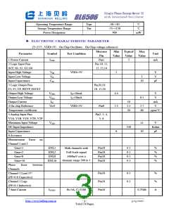
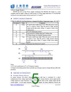
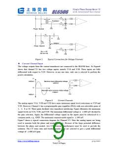
extract the real power component (i.e., the dc component), the instantaneous power signal is
low-pass filtered. Figure 2 illustrates the instantaneous real power signal and shows how the real
power information can be extracted by low-pass filtering the instantaneous power signal. This
scheme correctly calculates real power for non-sinusoidal current and voltage waveforms at all
power factors. All signal processing is carried out in the digital domain for superior stability over
temperature and time.
current
sampling
analog to
digital
high pass
filter
I
CF
F1
F2
digital
multipli-
cation
low pass
filter
digital to
frequency
integral
voltage
sampling
analog to
digital
high pass
filter
V
instantaneous real
power signal
instantaneous
power signal p(t)
V*I
p(t)=i(t)*v(t)
v(t)=V*cos(wt)
i(t)=I*cos(wt)
V*I
2
V*I
2
V*I
p(t)=
[1+cos(2wt)]
2
t
t
Figure 2.
Signal Processing Block Diagram
Accumulating this real power information generates the low frequency output of the BL6506. This
low frequency inherently means a long accumulation time between output pulses. The output
frequency is therefore proportional to the average real power. This average real power information
can, in turn, be accumulated (e.g., by a counter) to generate real energy information. Because of its
high output frequency and hence shorter integration time, the CF output is proportional to the
instantaneous real power. This is useful for system calibration purposes that would take place
under steady load conditions.
ꢀ
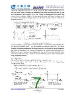
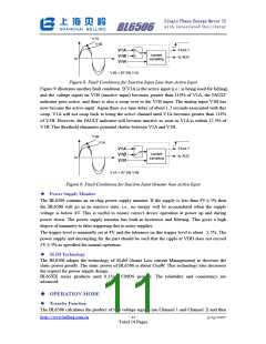
Offset Effect
The dc offsets come from the input signals and the forepart analog circuitry.
Assume that the input dc offsets on the voltage channel and the current channel are Uoffset and Ioffset
and PF equals 1 (φ=0).
,
p(t) = [U cos(
ω
t) + U offset ]× [I cos(
ω
t + Φ ) + I offset ]
UI
UI
=
+ Ioffset U cos(
ω
t) + U offset I cos(
ω
t) +
cos( 2ωt)
2
2
Figure 3.
Effect of Offset
- 7 -
http://www.belling.com.cn
3/15/2007
Total 14 Pages

 BELLING [ BELLING ]