SinglePhaseEnergyMeterIC
with Integrated Oscillator
BL6506
RF
CT
VAP
VN
+
-
CF
±660mV
RF
AGND
CF
AGND
AGND
Phase Neutral
CF
Ra
Rb
Rv
AGND
AGND
±660mV
VAP
VN
+
-
Phase Neutral
RF
AGND
CF
Ra >> RF
Rb+Rv=RF
AGND
AGND
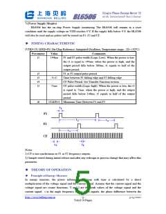
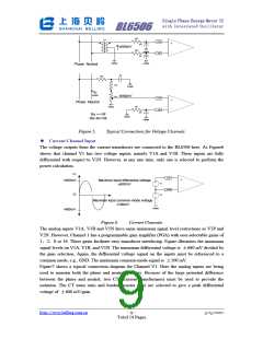
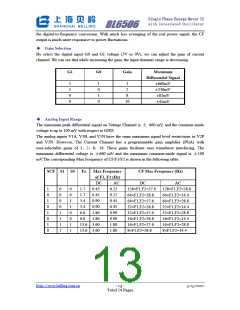
Figure 5.
Current Channel Input
Typical Connections for Voltage Channels
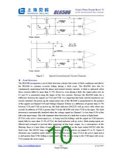
ꢀ
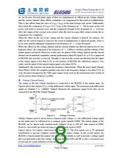
The voltage outputs from the current transducers are connected to the BL6506 here. As Figure6
shows that channel V1 has two voltage inputs, namely V1A and V1B. These inputs are fully
differential with respect to V1N. However, at any one time, only one is selected to perform the
power calculation.
V1
V2P
+
+660mV
Maximun input differential voltage
±660mV
V1
V2
-
V2N
V2
Maximun input common-mode voltage
±100mV
AGND
-660mV
Figure 6.
Current Channels
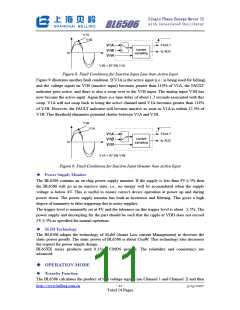
The analog inputs V1A, V1B and V1N have same maximum signal level restrictions as V2P and
V2N. However, Channel 1 has a programmable gain amplifier (PGA) with user-selectable gains of
1
,
2
,
8 or 16. These gains facilitate easy transducer interfacing. Figure illustrates the maximum
signal levels on V1A, V1B, and V1N. The maximum differential voltage is 660 mV divided by
the gain selection. Again, the differential voltage signal on the inputs must be referenced to a
common mode, e.g., GND. The maximum common-mode signal is 100 mV.
±
±
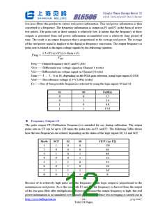
Figure7 shows a typical connection diagram for Channel V1. Here the analog inputs are being
used to monitor both the phase and neutral currents. Because of the large potential difference
between the phase and neutral, two CTs (current transformers) must be used to provide the
isolation. The CT turns ratio and burden resistor (Rb) are selected to give a peak differential
voltage of
±660 mV/gain.
http://www.belling.com.cn
- 9 -
3/15/2007
Total 14 Pages

 BELLING [ BELLING ]