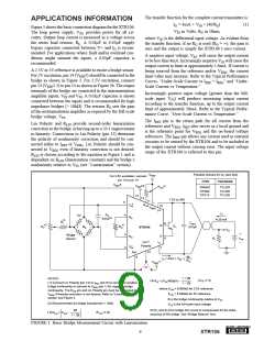
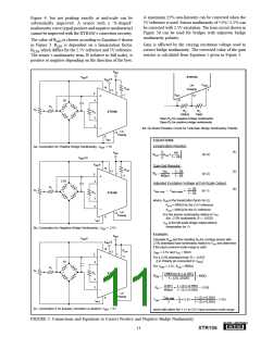
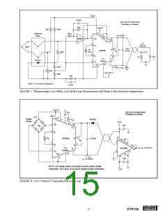
to the upper and lower sides of the bridge to keep the bridge
output within the 1.1V to 3.5V common-mode input range.
Bridge output is reduced so a preamplifier as shown may be
needed to reduce offset voltage and drift.
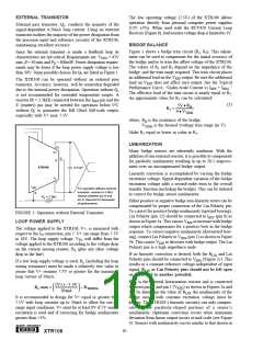
ERROR ANALYSIS
Table I shows how to calculate the effect various error
sources have on circuit accuracy. A sample error calculation
for a typical bridge sensor measurement circuit is shown
(5kΩ bridge, VREF = 5V, VFS = 50mV) is provided. The
results reveal the XTR106’s excellent accuracy, in this case
1.2% unadjusted. Adjusting gain and offset errors improves
circuit accuracy to 0.33%. Note that these are worst-case
errors; guaranteed maximum values were used in the calcu-
lations and all errors were assumed to be positive (additive).
The XTR106 achieves performance which is difficult to
obtain with discrete circuitry and requires less board space.
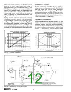
OTHER SENSOR TYPES
The XTR106 can be used with a wide variety of inputs. Its
high input impedance instrumentation amplifier is versatile
and can be configured for differential input voltages from
millivolts to a maximum of 2.4V full scale. The linear range
of the inputs is from 1.1V to 3.5V, referenced to the IRET
terminal, pin 6. The linearization feature of the XTR106 can
be used with any sensor whose output is ratiometric with an
excitation voltage.
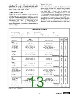
SAMPLE ERROR CALCULATION
Bridge Impedance (RB)
Ambient Temperature Range (∆TA)
Supply Voltage Change (∆V+)
5kΩ
20°C
5V
Full Scale Input (VFS
Excitation Voltage (VREF
Common-Mode Voltage Change (∆CM)
)
50mV
5V
25mV (= VFS/2)
)
ERROR
(ppm of Full Scale)
SAMPLE
ERROR EQUATION
ERROR SOURCE
ERROR CALCULATION
UNADJ
ADJUST
INPUT
Input Offset Voltage
vs Common-Mode
vs Power Supply
Input Bias Current
Input Offset Current
V
OS /V • 106
200µV/50mV • 106
50µV/V • 0.025V/50mV • 106
3µV/V • 5V/50mV • 106
50µV/V • 25nA • 2.5kΩ/50mV • 106
3nA • 5kΩ/50mV • 106
2000
25
0
25
300
0
FS
CMRR • ∆CM/V • 106
(V vs V+) • (∆V+)/V • 106
CMRR • IB • (RB /2)/ V • 106
FS
300
0.1
OS
FS
FS
IOS • RB /VFS • 106
300
2625
0
Total Input Error
325
EXCITATION
Voltage Reference Accuracy
vs Supply
V
REF Accuracy (%)/100% • 106
0.25%/100% • 106
2500
1
0
1
1
(VREF vs V+) • (∆V+) • (V /VREF
)
20ppm/V • 5V (50mV/5V)
FS
Total Excitation Error
2501
GAIN
Span
Span Error (%)/100% • 106
Nonlinearity (%)/100% • 106
0.2%/100% • 106
0.01%/100% • 106
2000
100
0
Nonlinearity
100
100
Total Gain Error
2100
OUTPUT
Zero Output
vs Supply
| IZERO – 4mA | /16000µA • 106
(IZERO vs V+) • (∆V+)/16000µA • 106
25µA/16000µA • 106
1563
62.5
1626
0
0.2µA/V • 5V/16000µA • 106
62.5
63
Total Output Error
DRIFT (∆TA = 20°C)
Input Offset Voltage
Input Offset Current (typical)
Voltage Refrence Accuracy
Span
Drift • ∆TA / (V ) • 106
1.5µV/ °C • 20°C / (50mV) • 106
5pA / °C • 20°C • 5kΩ/ (50mV) • 106
600
10
600
10
FS
Drift • ∆TA • RB / (V ) • 106
FS
35ppm/°C • 20°C
700
500
1125
2936
700
500
1125
2936
225ppm/°C • 20°C
Zero Output
Drift • ∆TA / 16000µA • 106
0.9µA/°C • 20°C / 16000µA • 106
Total Drift Error
NOISE (0.1Hz to 10Hz, typ)
Input Offset Voltage
Zero Output
V (p-p)/ V • 106
IZERO Noise / 16000µA • 106
[√ 2 • √ (RB / 2 ) / 1kΩ • 4nV / √ Hz • √10Hz ] / V • 106
0.6µV / 50mV • 106
0.035µA / 16000µA • 106
[√ 2 • √ 2.5kΩ / 1kΩ • 4nV/ √ Hz • √ 10Hz ] / 50mV • 106
(200fA/√Hz • 40.8 • √2 • 2.5kΩ)/50mV• 106
12
2.2
0.6
0.6
15
12
2.2
0.6
0.6
15
n
FS
Thermal RB Noise
Input Current Noise
FS
(in • 40.8 • √2 • RB / 2)/ V
•
106
FS
Total Noise Error
NOTE (1): All errors are min/max and referred to input, unless otherwise stated.
TOTAL ERROR:
11803
1.18%
3340
0.33%
TABLE I. Error Calculation.
®
13
XTR106

 BB [ BURR-BROWN CORPORATION ]