PCM1808
www.ti.com
SLES177A–APRIL 2006–REVISED AUGUST 2006
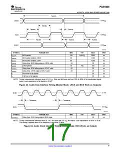
t
(LRCP)
0.5 V
DD
LRCK
t
(BCKL)
t
t
(CKLR)
(BCKH)
0.5 V
DD
BCK
t
t
t
(CKDO)
(LRDO)
(BCKP)
0.5 V
DD
DOUT
T0018-02
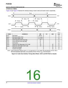
SYMBOL
PARAMETER
MIN
150
65
TYP
MAX
2000
1200
1200
20
UNIT
ns
t(BCKP)
BCK period
1/(64 fS)
t(BCKH)
t(BCKL)
t(CKLR)
t(LRCP)
t(CKDO)
t(LRDO)
tr
BCK pulse duration, HIGH
BCK pulse duration, LOW
ns
65
ns
Delay time, BCK falling edge to LRCK valid
LRCK period
–10
10
ns
1/fS
125
20
µs
Delay time, BCK falling edge to DOUT valid
Delay time, LRCK edge to DOUT valid
Rise time of all signals
–10
–10
ns
20
ns
20
ns
tf
Fall time of all signals
20
ns
NOTE: Timing measurement reference level is 0.5 VDD. Rise and fall times are from 10% to 90% of the input/output signal
swing. Load capacitance of all signals is 20 pF.
Figure 23. Audio Data Interface Timing (Master Mode: LRCK and BCK Work as Outputs)
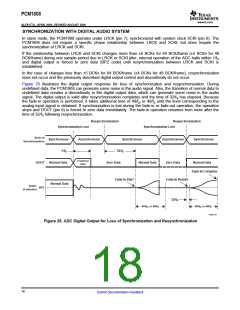
1.4 V
SCKI
t
t
(SCKBCK)
(SCKBCK)
0.5 V
BCK
DD
T0074-01
SYMBOL
PARAMETER
Delay time, SCKI rising edge to BCK edge
MIN
TYP
MAX
UNIT
ns
t(SCKBCK)
5
30
NOTE: Timing measurement reference level is 1.4 V for input and 0.5 VDD for output. Load capacitance of BCK is 20 pF.
This timing is applied when SCKI frequency is less than 25 MHz.
Figure 24. Audio Clock Interface Timing (Master Mode: BCK Works as Output)
17
Submit Documentation Feedback

 BB [ BURR-BROWN CORPORATION ]